Echelon I/O Model Reference for Smart Transceivers and Neuron Chips User Manual
Page 67

I/O Model Reference
57
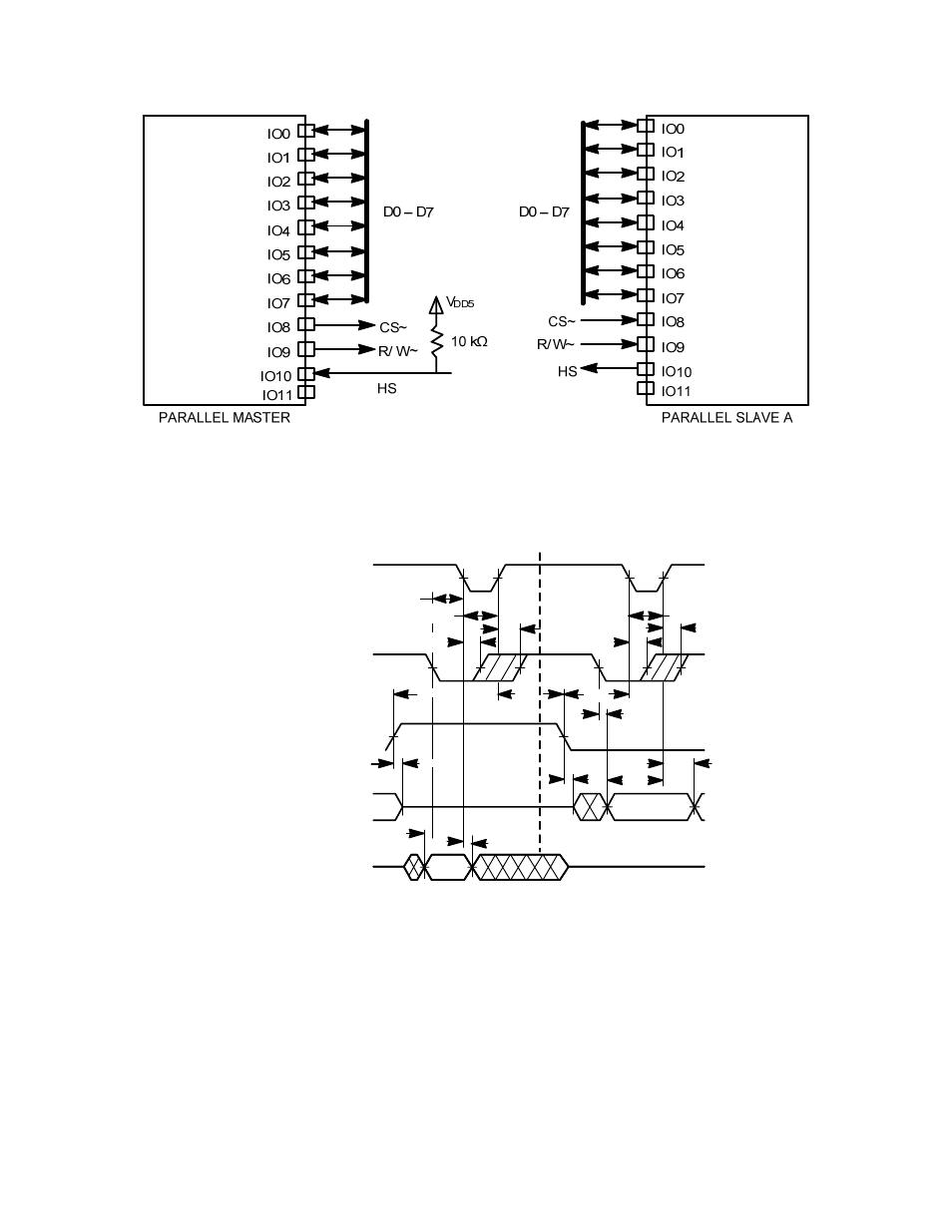
Figure 19. Master Mode and Slave A Mode
The maximum data transfer rate is 1 byte per 4 processor instruction cycles (2.4
μs per byte for a Series 3100 device with a 10 MHz input clock rate, or 300 ns per
byte for a Series 5000 device with an 80 MHz system clock). The data transfer
rate scales proportionally to the input clock rate (a master write is a slave read).
CS~
HS
DATA OUT
DATA IN
READ CYCLE
WRITE CYCLE
t
mhsv
t
mrws
t
mrdz
t
mwds
t
mhscs
t
mhsdv
t
mcspw
t
mhsh
R/W~
t
mrws
t
mhsh
t
mcspw
t
mrwh
t
mwdh
t
mwdd
t
mrdh
t
mrds
t
mhsv
Figure 20. Master Mode Timing
Timing for the case where the Smart Transceiver is the master (Table 21 on page
58), refers to measured output timing for a Series 3100 device at 10 MHz. After
every byte write or byte read, the HS line is monitored by the master, to verify
that the slave has completed processing (when HS = 0) and the slave is ready for
the next byte transfer. This is done automatically in Smart Transceiver-to-Smart
Transceiver (master/slave A mode) data transfers.
