Echelon I/O Model Reference for Smart Transceivers and Neuron Chips User Manual
Page 105

I/O Model Reference
95
DATA OUT
DATA IN
INPUT
CLOCK
TIME
t
ret
START
OF
io_in()
END OF
io_in()
DATA
OUTPUT
CLOCK
AND DATA
SAMPLED
DATA
OUTPUT
t
docki
t
cklodo
t
cklo
t
fin
CLOCK
SAMPLED
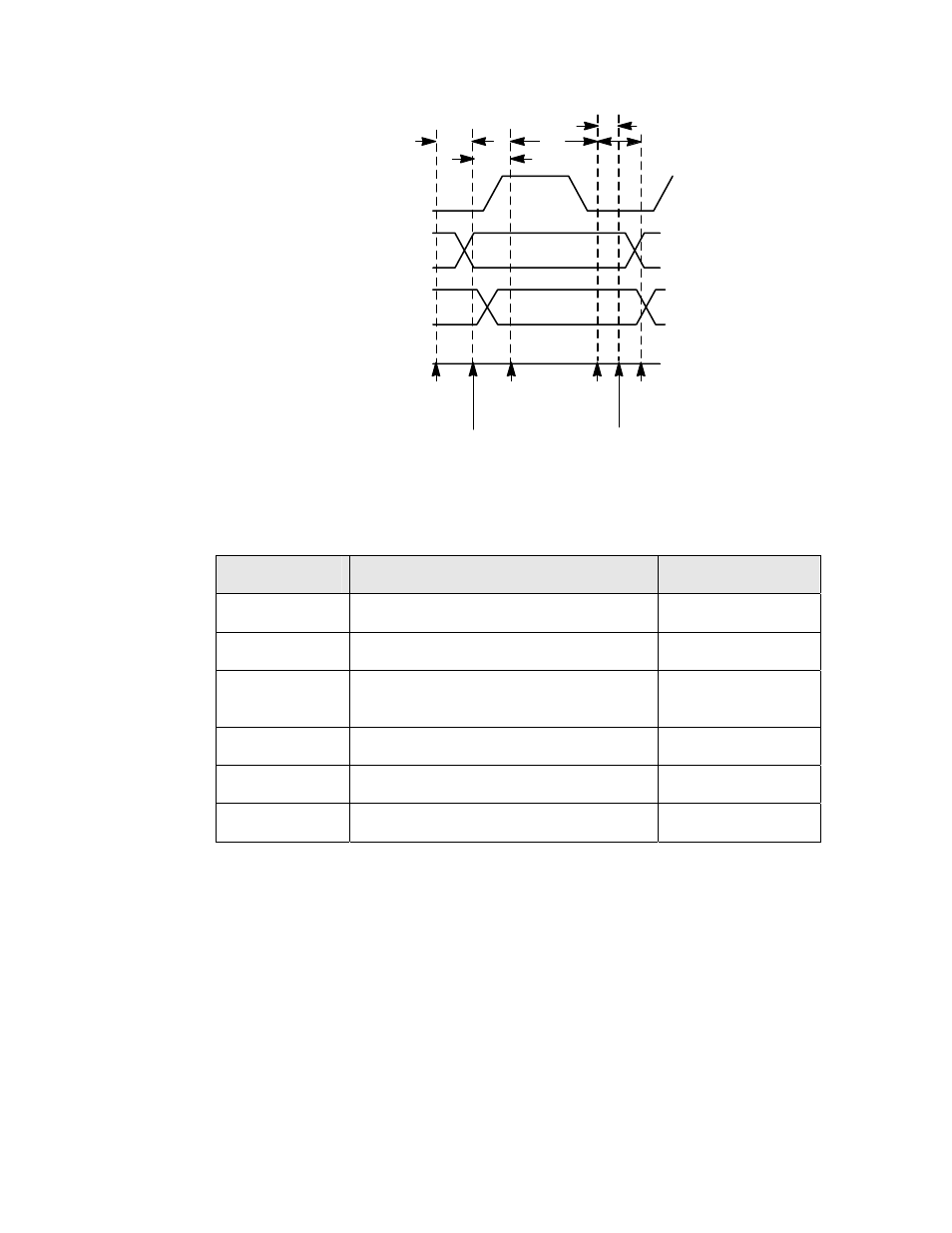
Figure 35. Neurowire Slave Timing
Table 36. Neurowire Slave Output Latency Values for Series 3100 Devices
Symbol
Description
Typical at 10 MHz
t
fin
Function call to data bit out
41.4 μs
t
ret
Return from function
19.2 μs
t
docki
Data out to input clock and data
sampled
4.8 μs
t
cklo
Data sampled to clock low sampled
24.0 μs
t
cklodo
Clock low sampled to data output
25.8 μs
f
Clock frequency (max)
18.31 kHz
The algorithm for each bit of output/input for the Neurowire slave objects is
described below. In this description, the default active clock edge (positive) is
assumed; if the invert keyword is used, all clock levels stated should be reversed.
1. Set IO9 to the next output bit value.
2. Test pin IO8, the clock input, for a high level (to test for the rising edge of
the input clock). If the input clock is still low, sample the timeout event
pin and abort if high.
3. When the input clock is high, store the next data input bit as sampled on
pin IO10.
4. Test the input clock for a low input level (to test for the falling edge of the
input clock). If the input clock is still high, sample the timeout event pin
and abort if high.
