Programming considerations – Echelon I/O Model Reference for Smart Transceivers and Neuron Chips User Manual
Page 129

I/O Model Reference
119
IO10
IO9
IO8
IO0
IO1
IO2
IO3
IO4
IO5
IO6
IO7
Optional Pull-Up Resistors
(3100 Family Only)
IO11
t
dw
DATA
A
START OF
io_in()
END OF
io_in()
DATA
B
TIMEOUT
TIME
t
ibd
t
fin
t
tow
t
tret
t
ret
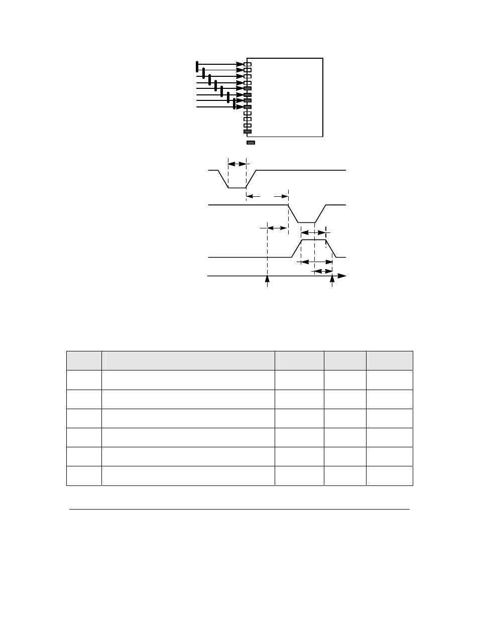
Figure 45. Wiegand Input and Timing
Table 47. Wiegand Input Latency Values for Series 3100 Devices
Symbol Description
Minimum
Typical
Maximum
t
fin
Function call to start of second data edge
—
75.6 μs —
t
dw
Input data width (at 10 MHz)
200 ns
100 μs 880
ms
t
ibd
Inter-bit
delay
150 μs — 900
μs
t
low
Timeout pulse width
—
39 μs —
t
tret
Timeout to function return
—
18.0 μs —
t
ret
Last data bit to function return
—
74.4 μs —
Programming Considerations
The wiegand I/O model is used to transfer data from a Wiegand format data
stream source. This format encodes data as a series of pulses on two signal lines:
