Muxbus input/output, Hardware considerations – Echelon I/O Model Reference for Smart Transceivers and Neuron Chips User Manual
Page 62

52
Parallel I/O Models
Muxbus Input/Output
The multiplexed bus (muxbus) I/O model provides a means of performing parallel
I/O data transfers between a Smart Transceiver and an attached peripheral
device or processor. This I/O model allows you to interface with any device that
requires an address and a data bus, such as a programmable universal
asynchronous receiver/transmitter (UART).
The muxbus I/O model uses eleven I/O pins to form an 8-bit address and bi-
directional data bus interface. This I/O model uses pins IO_0 through IO_7 for
the 8-bit address bus and the 8-bit data bus. Pins IO_8 through IO_10 are
control signals that are always driven by the Neuron Chip or Smart Transceiver,
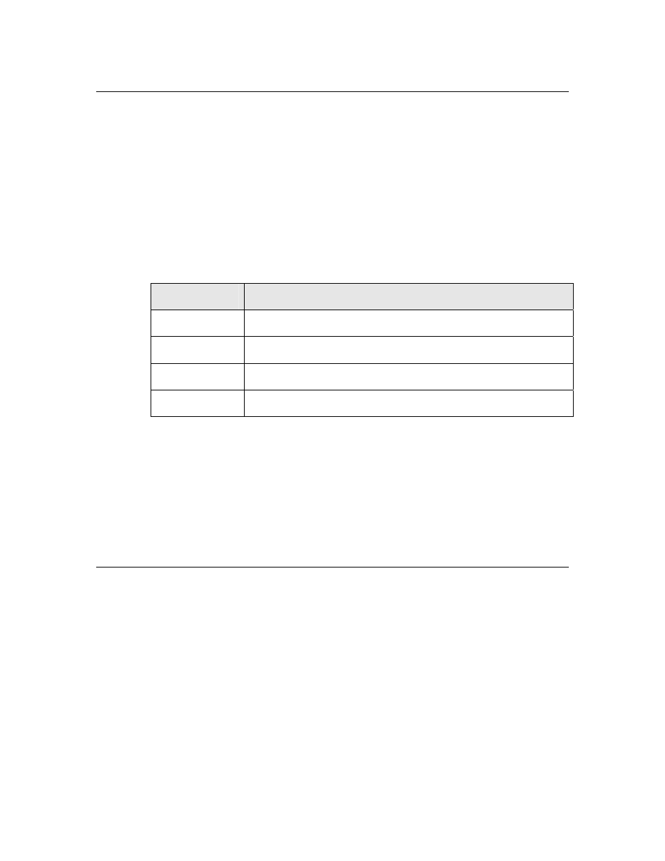
as shown in Table 19.
Table 19. Muxbus Signals
Pin
Function
IO0 thru IO7
Address and bi-directional data
IO_8
C_ALS: Address latch strobe, asserted high
IO_9
C_WS~: Write strobe, asserted low
IO_10
C_RS~: Read strobe, asserted low
This I/O model provides the capability to build an 8-bit data bus system with an
8-bit address bus. Typically, an 8-bit D-type latch (such as a 74HC573) is
connected to the Neuron I/O pins where pins IO_0 through IO_7 are connected to
the eight Q inputs. Pin IO_8 is connected to the Latch Enable input. In this
configuration, eight bits of address are latched on the eight D output pins of the
74HC573 device.
Pins IO_9 and IO_10 are the write and read strobes, normally high.
This model applies to Series 3100 Neuron Chips and Smart Transceivers, and to
Series 5000 Neuron Processors and Smart Transceivers.
Hardware Considerations
Unlike the parallel input/output model, which uses a token-passing scheme for
ensuring synchronization, the muxbus input/output enables a Smart Transceiver
to essentially be in control of all read and write operations at all times. This
control relieves the burden of protocol handling from the attached device and
results in an easier-to-use interface at the expense of data throughput capacity.
The data bus remains in the last state used.
Figure 18 on page 53 shows the muxbus I/O latency times. These are the times
from the call to the io_in() or io_out() function, until a value is returned. The
direction of bit ports can be changed between input and output dynamically by
using the io_set_direction() function.
