Echelon I/O Model Reference for Smart Transceivers and Neuron Chips User Manual
Page 21

I/O Model Reference
11
used by the application are tied high or low on the PC board, or are left
unconnected and configured as a bit output by the application in order to prevent
unnecessary power consumption. See the
PL 3120 / PL 3150 / PL 3170 Power
Line Smart Transceiver Data Book
for more information.
For Series 5000 devices, the I/O pins do not have configurable pull-ups or high
current-sink capability. If your I/O circuitry requires pull-up resistors, you must
add them to the hardware design for the device. The I/O pins on a Series 5000
device have an 8 mA current source and sink capability. If your I/O circuitry has
higher current requirements, you can add external driver circuitry (for example,
using a Fairchild Semiconductor
®
74AC245/74ACT245 Octal Bidirectional
Transceiver or 74VHC245/74VHCT245 Octal Buffer/Line Driver).
In addition, the Series 5000 device pins are all 3.3 V pins: the input pins are 5 V
tolerant, and the output pins are CMOS compatible. Series 3100 device pins are
all 5 V pins.
For both Series 3100 and Series 5000 devices, pins IO0 – IO7 have low-level
detect latches.
Because the I/O pins are controlled by system firmware, the timing for reading or
writing an I/O pin includes latency that can vary by I/O model and even vary by
I/O pin. All inputs are software sampled during processing for the Neuron C
when statement. In general, the latency scales inversely with the system clock
rate.
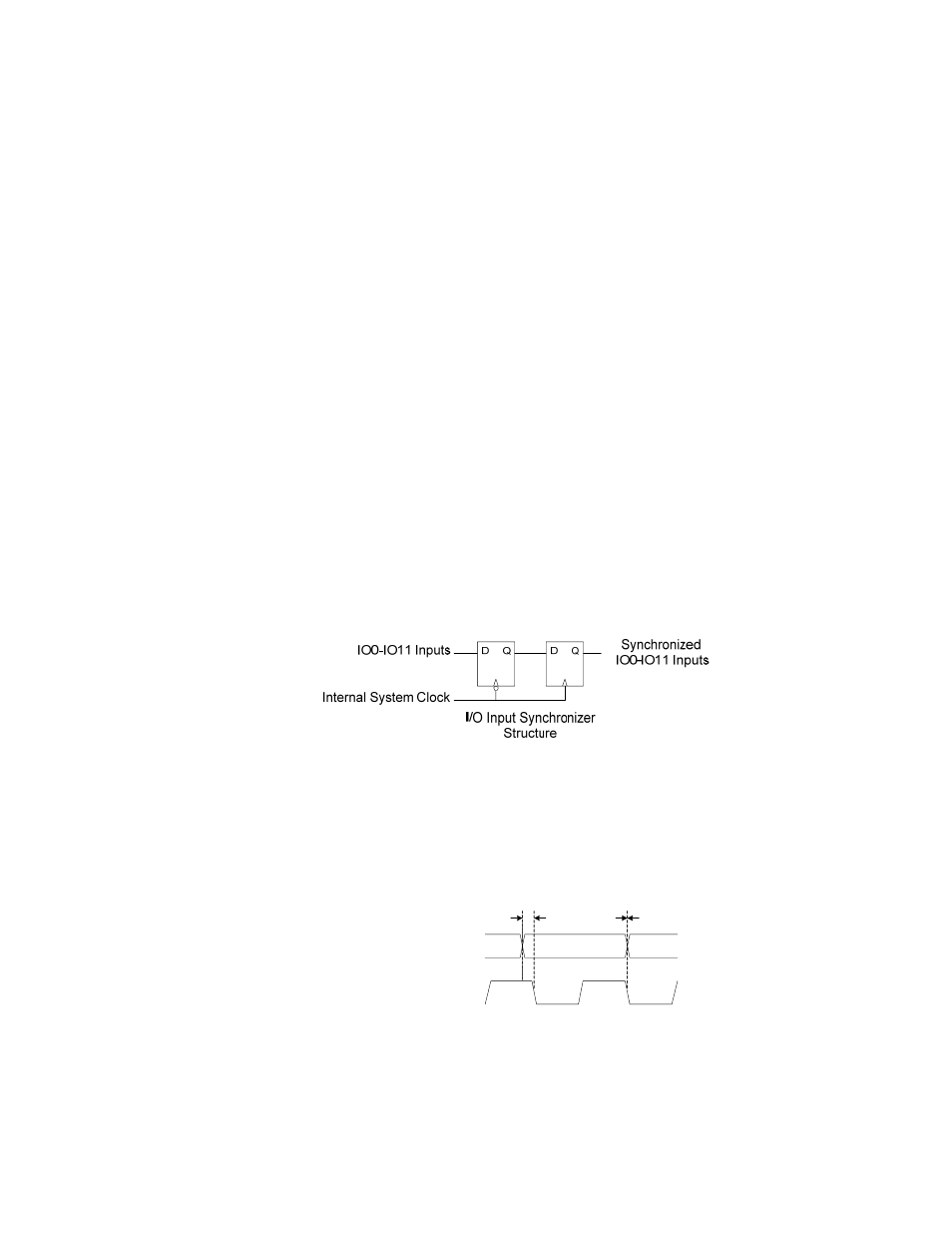
To maintain and provide consistent behavior for external events, and to prevent
setup and hold metastability, all I/O pins, when configured as simple inputs, are
passed through a hardware synchronization block, shown in Figure 2, that is
sampled by the internal system clock.
Figure 2. Synchronization Block
I/O pins used for other functions do not have this synchronization requirement.
For Series 3100 devices, the sample rate is always the input clock divided by two
(for example, for a 10 MHz input clock, the sample rate is 5 MHz). For a signal to
be reliably synchronized with a 10 MHz input clock, it must be at least 220 ns in
duration; see Figure 3.
Internal System
Clock
(XIN Input Clock
10 MHz divided by 2)
IO0-IO11 Inputs
(220 ns pulse)
t
setup
20 ns
t
hold
0 ns
Figure 3. Synchronization of External Signals for Series 3100 Devices
