Echelon I/O Model Reference for Smart Transceivers and Neuron Chips User Manual
Page 51

I/O Model Reference
41
The direction of nibble ports can be changed between input and output
dynamically under application control (see
on page
42). The least-significant bit (LSB) of the input data is determined by the object
declaration and can be any of the IO0 – IO4 pins.
For Series 3100 devices, the high (20 mA) current sink capability of pins IO0 –
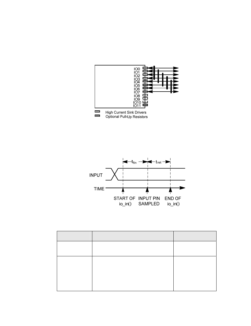
IO3 (see Figure 14) allows these pins to drive many I/O devices directly.
Figure 14. Nibble Input/Ouput
Figure 15 and Figure 16 on page 42 show the nibble input and nibble output
latency times, respectively. These are the times from the call to the io_in() or
io_out() function, until a value is returned. The direction of bit ports can be
changed between input and output dynamically by using the io_set_direction()
function.
Figure 15. Nibble Input Timing
Table 16. Nibble Input Latency Values for Series 3100 Devices
Symbol
Description
Typical at 10 MHz
t
fin
Function call to sample
IO0 – IO4
41 μs
t
ret
Return from function
IO0
IO1
IO2
IO3
IO4
18 μs
22.8 μs
27.5 μs
32.3 μs
36 μs
