Figure 26, 77 an – Echelon I/O Model Reference for Smart Transceivers and Neuron Chips User Manual
Page 87

I/O Model Reference
77
DATA IN
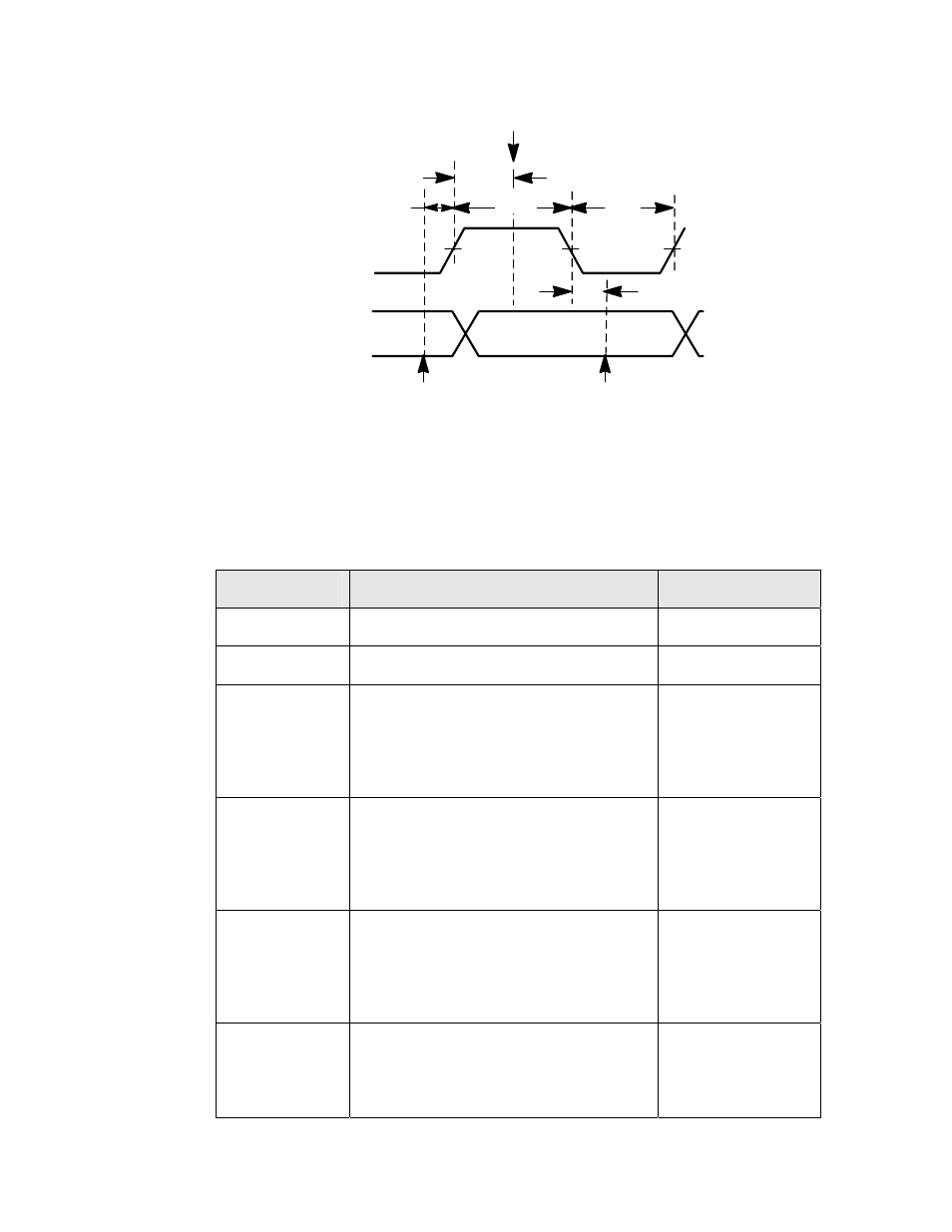
Active clock edge assumed to be positive in the above diagram.
OUTPUT
CLOCK
INPUT SAMPLED
END OF
io_in()
START OF
io_in()
t
hold
t
fin
t
tae
t
ret
t
aet
Figure 26. Bitshift Input Timing
Table 30. Bitshift Input Latency Values for Series 3100 Devices
Symbol
Description
Typical at 10 MHz
t
fin
Function call to first edge
156.6 μs
t
ret
Return from function
5.4 μs
t
hold
Active clock edge to sampling of input
data
15 kbps bit rate
10 kbps bit rate
1 kbps bit rate
9 μs
40.8 μs
938.2 μs
t
aet
Active clock edge to next clock
transition
15 kbps bit rate
10 kbps bit rate
1 kbps bit rate
31.8 μs
63.6 μs
961 μs
t
tae
Clock transition to next active clock
edge
15 kbps bit rate
10 kbps bit rate
1 kbps bit rate
14.4 μs
14.4 μs
14.4 μs
f
Clock frequency = 1/(t
aet
+ t
tae
)
15 kbps bit rate
10 kbps bit rate
1 kbps bit rate
21.6 kHz
12.8 kHz
1.03 kHz
