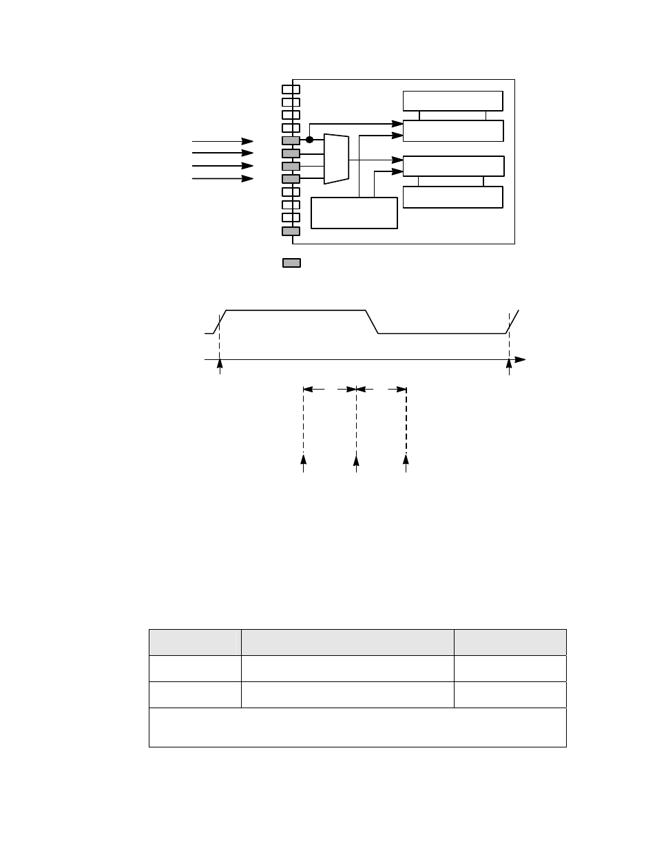
Figure 53 – Echelon I/O Model Reference for Smart Transceivers and Neuron Chips User Manual
Page 153

I/O Model Reference
143
READ
TIMER/
COUNTER
FLAG AND
EVENT
REGISTER
CLEAR FLAG
END OF
io_in()
START OF
io_in()
STOP TIMER
COUNTER
START TIMER
COUNTER
TIME
INPUT
t
fin
t
ret
mux
Event Register
IO10
IO9
IO8
IO0
IO1
IO2
IO3
IO4
IO5
IO6
IO7
System Clock
Divide Chain
Optional Pull-Up Resistors for 3100 Family Devices
Event Register
Timer/Counter 2
Timer/Counter 1
IO11
Figure 53. Period Input and Timing
Table 54. Period Input Latency Values for Series 3100 Devices
Symbol
Description
Typical at 10 MHz
t
fin
Function call to input sample
86 μs
t
ret
Return from function
52 μs or 22 μs
Note: If the measurement is new, t
ret
= 52 μs. If a new time is not being
returned, t
ret
= 22 μs.
