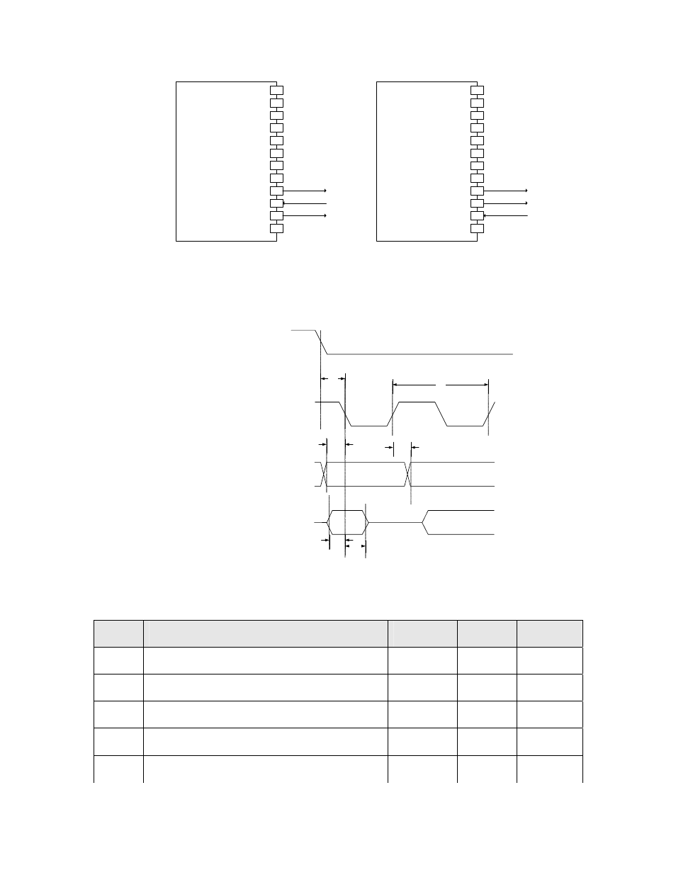
Clock cycle (user specified) — — — t, Select low to clock transition 4.8 μs — — t, Data out to clock (1st bit of invert mode) 0.5 * t – Echelon I/O Model Reference for Smart Transceivers and Neuron Chips User Manual
Page 122: Clock to data out — — 5 ns t, Data in setup 10 ns, Spi master, Spi master (neurowire pin mode), Figure 41. spi master mode i/o, Figure 42. spi master mode timing

112
Serial I/O Models
Table 44. SPI Master Mode I/O Latency Values for Series 3100 Devices
Symbol Description
Minimum
Typical
Maximum
T
ck
Clock cycle (user specified)
—
—
—
T
sc
Select low to Clock transition
4.8 μs — —
T
doc
Data out to Clock (1st bit of invert mode)
0.5 * T
ck
—
—
T
cdo
Clock to data out
—
—
5 ns
T
dis
Data in setup
10 ns
—
—
IO0
IO10
IO9
IO8
IO7
IO6
IO5
IO4
IO3
IO2
IO1
IO11
SPI Master
IO0
IO10
IO9
IO8
IO7
IO6
IO5
IO4
IO3
IO2
IO1
IO11
SPI Master (Neurowire
pin mode)
Clock
MISO
MOSI
Clock
Data Out
Data In
Figure 41. SPI Master Mode I/O
Tcdo
Clock
(invert for
clockedge+
or
invert=true)
Data Out
Data In
Select
Tdis
Tdih
Tsc
Tdoc
Tck
Figure 42. SPI Master Mode Timing
