Programming considerations, Syntax, Figure 16 on – Echelon I/O Model Reference for Smart Transceivers and Neuron Chips User Manual
Page 52: 42 sh

42
Direct I/O Models
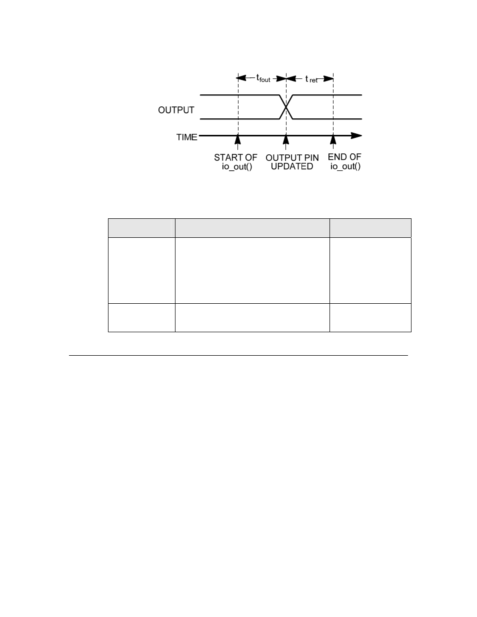
Figure 16. Nibble Output Timing
Table 17. Nibble Output Latency Values for Series 3100 Devices
Symbol
Description
Typical at 10 MHz
t
fout
Function call to update
IO0
IO1
IO2
IO3
IO4
78 μs
89.8 μs
101.5 μs
113.5 μs
125 μs
t
ret
Return from function
IO0 – IO4
5 μs
Programming Considerations
For nibble input/output, the data type of
return_value
for the io_in( ) function,
and the data type of the output value for the io_out( ) function is an unsigned
short.
For Series 3100 devices, add a #pragma enable_io_pullups directive to enable the
Neuron Chip’s or Smart Transceiver's built-in pull-up resistors on pins IO_4
through IO_7.
Syntax
pin
input nibble
io-object-name
;
pin
output nibble
io-object-nam
e [=
initial-output-level
];
pin
An I/O pin. Nibble input/output requires four adjacent pins. The pin
specification denotes the lowest numbered pin of the set and can be IO_0
