Echelon I/O Model Reference for Smart Transceivers and Neuron Chips User Manual
Page 120

110
Serial I/O Models
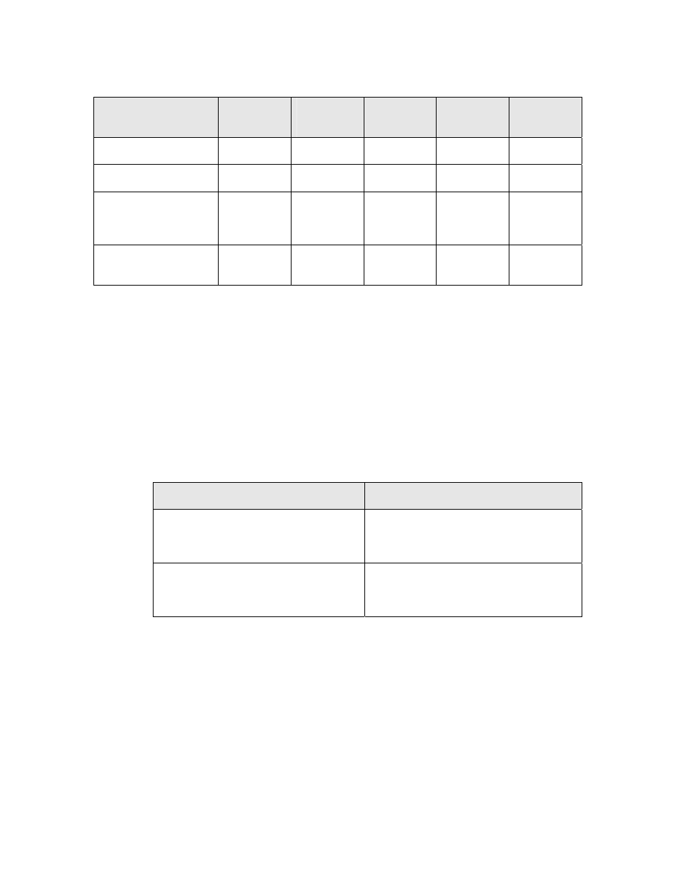
Table 42. SPI Slave Mode for Series 5000 Devices
Parameter
Value for
80 MHz
Value for
40 MHz
Value for
20 MHz
Value for
10 MHz
Value for
5 MHz
Max burst rate
10 Mbps
5 Mbps
2.5 Mbps
1.25 Mbps
625 kbps
Max burst size
16 bytes
16 bytes
16 bytes
16 bytes
16 bytes
Min burst spacing
(from start of one
burst to next)
100 μs 200
μs 400
μs 800
μs 1600
μs
Max sustained data
rate
430 kbps
210 kbps
100 kbps
40 kbps
25 kbps
Sustained reception in slave mode at high bit rates can starve the application
processor and cause overruns, and presents a possible risk of watchdog timeout.
Care must be given to allow the Smart Transceiver to process received bytes in a
timely manner. Master mode has no such restriction because the Smart
Transceiver regulates the data transfer.
The clockedge and invert keywords are used to determine the point at which data
is sampled and the idle level of the clock signal. By default, the clock signal is
idle at the logic 1 level. Use the invert keyword to change the idle state to
correspond to a logic 0 level. Common SPI implementations use the terms clock
phase (CPHA) and clock polarity (CPOL) to determine the behavior of the clock
signal during SPI transmissions. These terms relate directly to the clockedge
and invert keywords used in the I/O object declaration, as described in Table 43.
Table 43. Relating CPHA and CPOL to Neuron C Declarations
SPI Clock Signal State
Neuron C Declaration
CPHA
0
1
clockedge(-)
clockedge(+)
CPOL
0
1
invert
[default]
The active edge of the clock is determined by the clockedge and invert keywords.
If the clock signal is idle at logic 1 (default), then clockedge(-) indicates that the
falling edge of the clock signal is active. If the invert keyword is used, the rising
edge of the clock signal would be active (see Figure 39 and Figure 40 on page
111). In-phase interfaces (CPHA=1) present the data bit on the first transition of
the clock signal, and latch it on the second transition. Out-of-phase interfaces
(CPHA=0) present the data bit before the first transition of the clock signal, and
latch it on the first transition.
