Echelon I/O Model Reference for Smart Transceivers and Neuron Chips User Manual
Page 114

104
Serial I/O Models
Parity is not supported for this model. The application code can use bit I/O pins
for flow control handshaking if required.
STA
R
T
STA
R
T
STO
P
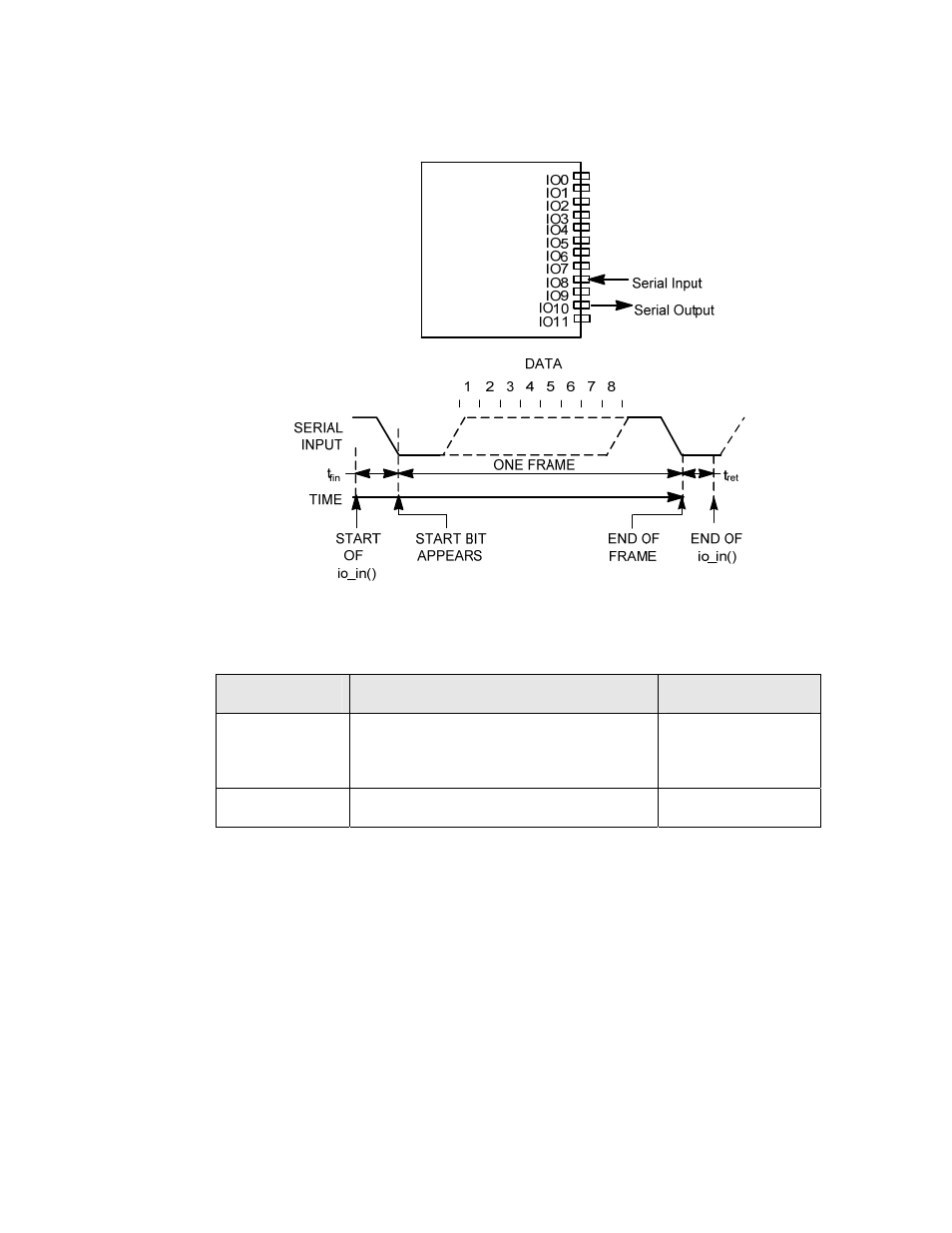
Figure 37. Serial Input and Timing
Table 37. Serial Input Latency Values for Series 3100 Devices
Symbol
Description
Typical at 10 MHz
t
fin
Function call to input sample
Min (first sample)
Max (timeout)
67 μs
20 byte frame
t
ret
Return from function
10 μs
The duration of this function call is a function of the number of data bits
transferred and the transmission bit rate. t
fin
(max) refers to the maximum
amount of time this function waits for a start bit to appear at the input. After
this time, the function returns a 0 as data. t
fin
(min) is the time to the first
sampling of the input pin. For example, the timeout period at 2400 bits/second is
(20 x 10 x 1/2400) + t
fin
(min).
