2 gpio port 2 register descriptions, 1 gpio direction register port 2 (pd2), 2 gpio output register port 2 (po2) – Maxim Integrated MAX31782 User Manual
Page 99: 3 gpio input register for port 2 (pi2), 11 .2 gpio port 2 register descriptions -5, 2gpioport2registerdescriptions, 1gpiodirectionregisterport2(pd2), 2gpiooutputregisterport2(po2), 3gpioinputregisterforport2(pi2)
MaximIntegrated 11-5
MAX31782 User’s Guide
Revision 0; 8/11
11.2GPIOPort2RegisterDescriptions
Port 2 provides eight GPIO pins that are multiplexed with the tachometers and master I
2
C port . This port does not
provide GPIO interrupts .
The tachometer function is an alternate function . This means that the GPIO functions are fully supported, even when the
pin is operating as a tachometer . If the tachometer is enabled while the pin is being operated as an output GPIO pin,
a high-to-low output transition is monitored by the tachometer and can cause a tachometer interrupt . The tachometer
functionality is disabled by setting the TACHCNn .TEXEN bit to a 0, where n = 0 to 5 .
GPIO pins P2 .6 and P2 .7 are multiplexed with the master I
2
C port . The master I
2
C port is a special function and disables
GPIO output when enabled (I2CCN_M .I2CEN = 1) . These two pins are open-drain output pins and do not have the
p-channel drive transistor or weak internal pullup . An external pullup resistor is required to achieve a high-logic level .
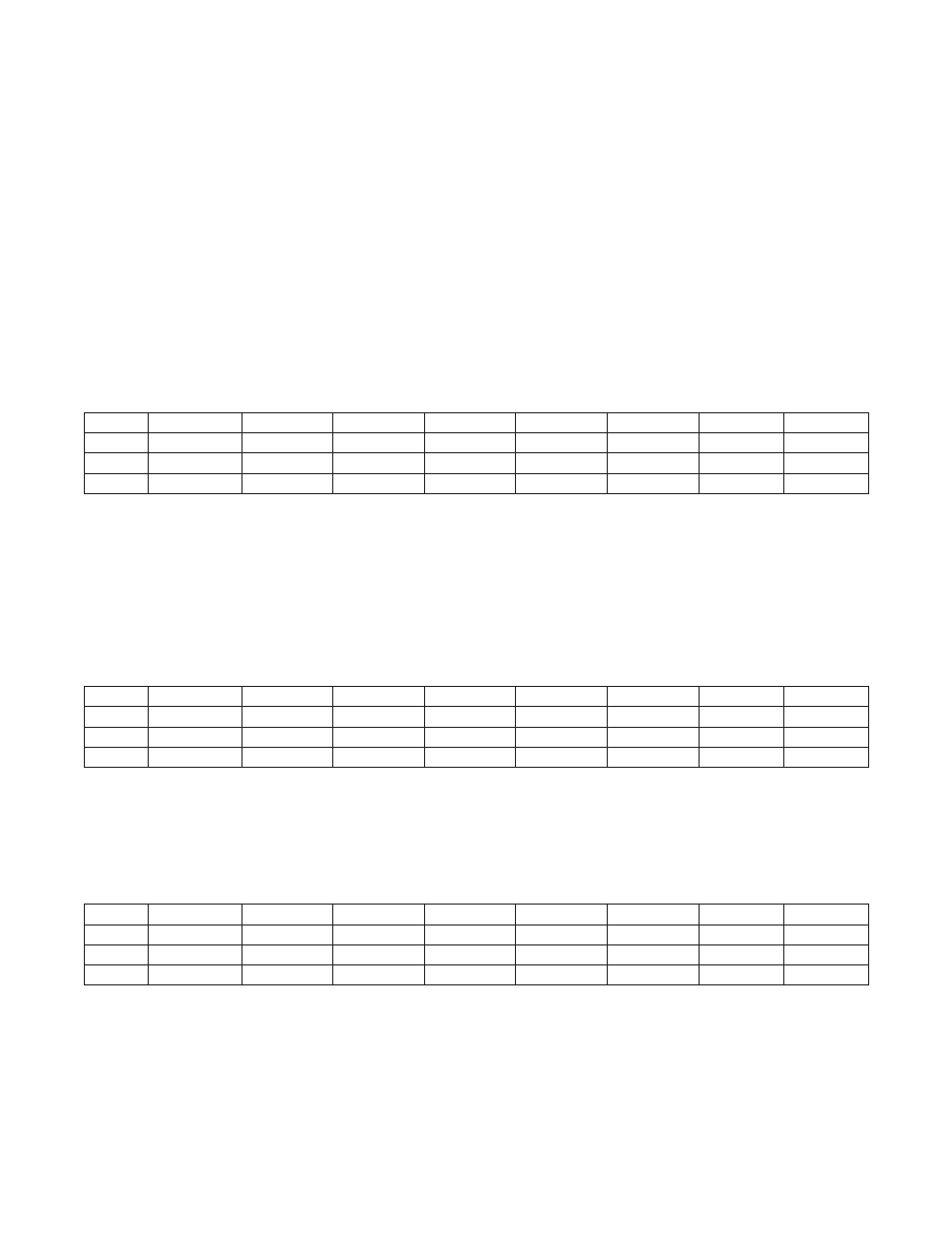
11.2.1GPIODirectionRegisterPort2(PD2)
PD2 is an 8-bit register used to determine the direction of the pins when they are used as GPIO pins . Each pin is inde-
pendently controlled by its direction bit . When PD2 .n (n = 0 to 7) is set to 1, the pin is an output; data in the PO2 .n bit
is driven on the pin . When PD2 .n is cleared to 0, the pin is an input, and allows an external signal to drive the pin . Note
that each port pin has a weak pullup circuit when functioning as an input . The p-channel pullup transistor is controlled
by the PO2 .n bit . If PO2 .n is set to 1, the corresponding weak pullup is turned on; if the PO2 .n bit is cleared to 0, the
weak pullup is turned off and the pin’s input is high impedance . The weak pullup transistor is not available on pins P2 .6
and P2 .7 .
11.2.2GPIOOutputRegisterPort2(PO2)
PO2 is an 8-bit register that controls the output data of a GPIO pin . If the pin is setup to be an output (PD2 .n = 1), the
data in PO2 .n is output on the pin . If the pin is set as an input (PD2 .n = 0), setting PO2 .n to a 1 enables a p-channel
weak pullup, otherwise the pin’s input is high impedance . If the P2 .6 and P2 .7 pins (master I
2
C port) are driven as an
output, they operate as open-drain outputs . An external pullup resistor is required to achieve a high-logic level .
11.2.3GPIOInputRegisterforPort2(PI2)
PI2 is an 8-bit register that contains the data that is applied to the GPIO pins . The PI2 input register contains valid input
data even when the pin is not operating as a GPIO . The reset value for this register is dependent on the logical states
applied to the pins . Note that each pin, except P2 .6 and P2 .7, has a weak pullup circuit when functioning as an input,
and the p-channel pullup transistor is controlled by the PO2 .n bit .
Bit
7
6
5
4
3
2
1
0
Name
PD2_7
PD2_6
PD2_5
PD2_4
PD2_3
PD2_2
PD2_1
PD2_0
Reset
0
0
0
0
0
0
0
0
Access
rw
rw
rw
rw
rw
rw
rw
rw
Bit
7
6
5
4
3
2
1
0
Name
PO2_7
PO2_6
PO2_5
PO2_4
PO2_3
PO2_2
PO2_1
PO2_0
Reset
1
1
1
1
1
1
1
1
Access
rw
rw
rw
rw
rw
rw
rw
rw
Bit
7
6
5
4
3
2
1
0
Name
PI2_7
PI2_6
PI2_5
PI2_4
PI2_3
PI2_2
PI2_1
PI2_0
Reset
s
s
s
s
s
s
s
s
Access
r
r
r
r
r
r
r
r