3 gpio port 6 register descriptions, 1 gpio direction register port 6 (pd6), 2 gpio output register port 6 (po6) – Maxim Integrated MAX31782 User Manual
Page 100: 11 .3 gpio port 6 register descriptions -6, 3gpioport6registerdescriptions, 1gpiodirectionregisterport6(pd6), 2gpiooutputregisterport6(po6)
MaximIntegrated 11-6
MAX31782 User’s Guide
Revision 0; 8/11
11.3GPIOPort6RegisterDescriptions
Port 6 provides seven GPIO pins that are multiplexed with the test access port (TAP), Timer B, and slave I
2
C port . See
for more details about the multiplexed functions and how to enable or disable these functions .
Note that SCL and SDA pins can be configured as GPIOs (P6 .6 and P6 .7, respectively) with open drain if needed,
although this is not the typical application . In this case, bits 6 and 7 in the port 6 SFRs control the GPIO functions of
the SCL and SDA pins, respectively . SCL and SDA are open-drain outputs and do not have the p-channel drive tran-
sistor or weak internal pullup . External pullups are required to realize a logic-high . The user should also be aware that
once SCL and SDA are converted to GPIO, they can no longer perform I
2
C communications . The host cannot talk to
the device through the I
2
C-compatible slave interface or use the I
2
C bootloader . See the
for more information .
On device reset, the TAP port is active, allowing for in-circuit debugging and programming . The TAP TDO pin (P6 .3) is
a logic-high output following a device reset . Extra precautions must be taken to ensure that this pin does not cause any
undesirable operations following a reset .
Port 6 also provides GPIO interrupts on all the pins . A GPIO interrupt can be generated when the pin is being operated
as a GPIO, or a special or alternate function . Three additional registers—EIF6, EIE6, and EIES6—are used to control
the GPIO interrupts .
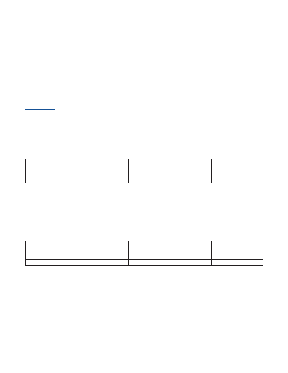
11.3.1GPIODirectionRegisterPort6(PD6)
PD6 is an 8-bit register used to determine the direction of the pins when they are used as GPIO pins . Each pin is
independently controlled by its direction bit . When PD6 .n (n = 0 to 7 excluding 5) is set to 1, the pin is an output; data
in the PO6 .n bit is driven on the pin . When PD6 .n is cleared to 0, the pin is an input, and allows an external signal to
drive the pin . Note that each port pin except P6 .6 and P6 .7 has a weak pullup circuit when functioning as an input . The
p-channel pullup transistor is controlled by the PO6 .n bit . If PO6 .n is set to 1, the corresponding weak pullup is turned
on; if the PO6 .n bit is cleared to 0, the weak pullup is turned off and the pin’s input is high impedance . The weak pullup
transistor is not available on pins P6 .6 and P6 .7 .
11.3.2GPIOOutputRegisterPort6(PO6)
PO6 is an 8-bit register that controls the output data of a GPIO pin . If the pin is set up to be an output (PD6 .n = 1), the
data in PO6 .n is output on the pin . If the pin is set as an input (PD6 .n = 0), setting PO6 .n to a 1 enables a p-channel
weak pullup; otherwise, the pin’s input is high impedance . If the P6 .6 and P6 .7 pins (slave I
2
C port) are driven as an
output, they operate as open-drain outputs . An external pullup resistor is required to achieve a high-logic level .
Bit
7
6
5
4
3
2
1
0
Name
PD6_7
PD6_6
—
PD6_4
PD6_3
PD6_2
PD6_1
PD6_0
Reset
0
0
0
0
0
0
0
0
Access
rw
rw
r
rw
rw
rw
rw
rw
Bit
7
6
5
4
3
2
1
0
Name
PO6_7
PO6_6
—
PO6_4
PO6_3
PO6_2
PO6_1
PO6_0
Reset
1
1
1
1
1
1
1
1
Access
rw
rw
r
rw
rw
rw
rw
rw