4 clock output mode, 12 .1 .4 clock output mode -6, Figure 12-4 . clock output mode block diagram -6 – Maxim Integrated MAX31782 User Manual
Page 108: 4clockoutputmode
MaximIntegrated 12-6
MAX31782 User’s Guide
Revision 0; 8/11
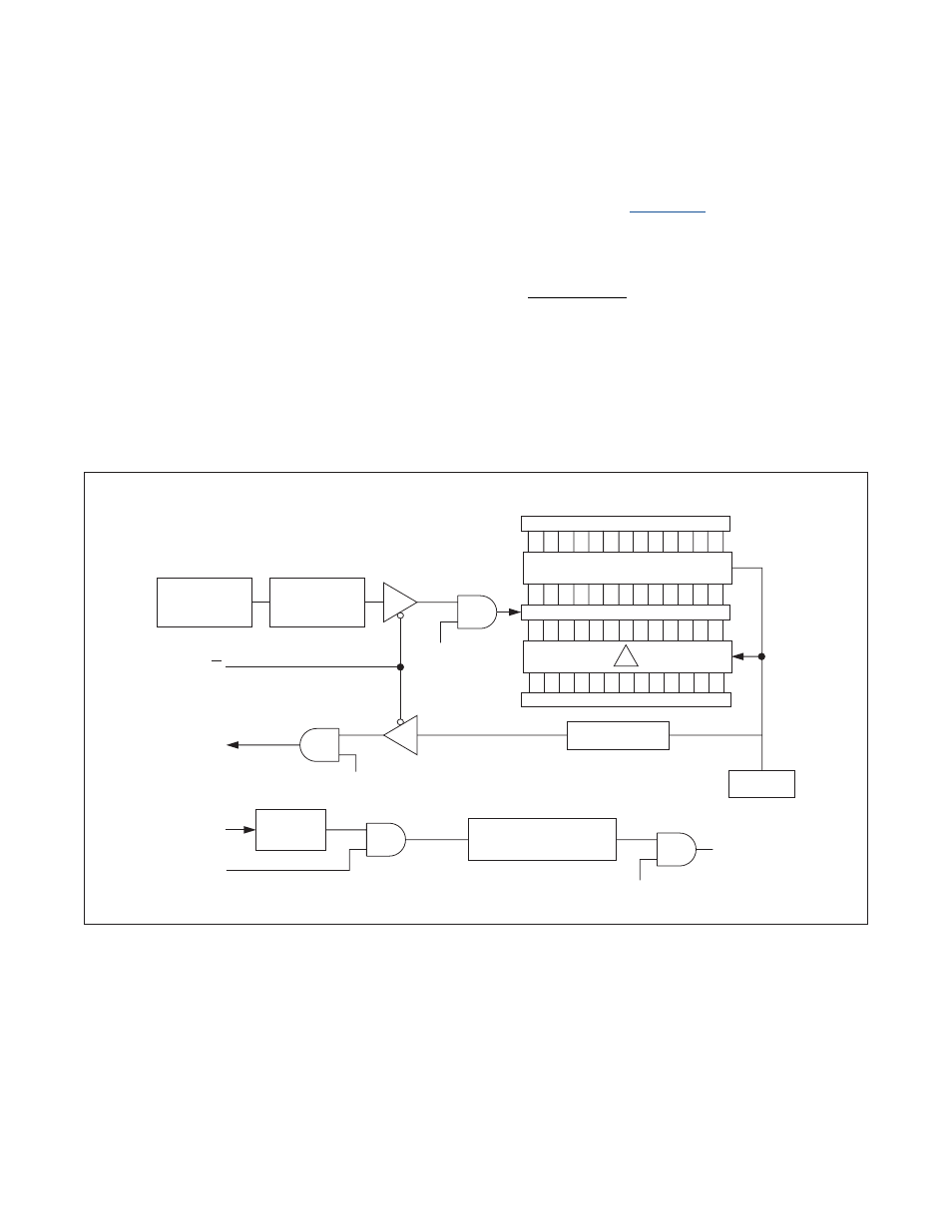
12.1.4ClockOutputMode
The Timer B can be configured to drive a clock output on the TBA pin as shown in
. For the timer to operate
in this mode, the capture/reload select bit (CP/RLB) and the counter/timer select bit (C/TB) must be cleared to 0 and the
Timer B output enable bit (TBOE) must be set to 1 . In this mode, the DCEN bit has no effect . The clock signal output is
a 50% duty cycle square wave with a frequency given by the equation:
TBA OUTPUT FREQUENCY =
TIMER B Clock
2 (TB0R 1)
×
+
where Timer B clock is the prescaled version of the system clock . The prescaler is set using the TBPS[2:0] bits . In clock
output mode, the setting of the TFB overflow flag does not cause an interrupt .
For example, if the Timer B clock is 1MHz and the TB0R register is set to 0004h, the TBA output frequency is 100kHz .
When the Timer B is operating in clock output mode, it can also monitor and generate an interrupt when falling edges
occur on the TBB pin . This is enabled by setting the EXENB and ETB bits .
Figure 12-4. Clock Output Mode Block Diagram
SYSTEM
CLOCK
FALLING
EDGE
CLOCK PRESCALER
TBPS[2:0]
TRB
TB0R
TB0V
0000h
COMPARE
DIVIDE BY 2
TFB = 1
TIMER B
INTERRUPT
EXFB = 1
TBOE
ETB
CLK
0
15
0
15
C/TB
TBA PIN
EXENB
TBB PIN