2 adc data buffer (addata when adcfg = 0), Table 6-3 . adc data bit weighting -9, Table6-3.adcdatabitweighting – Maxim Integrated MAX31782 User Manual
Page 52: 2adcdatabuffer(addatawhenadcfg=0)
MaximIntegrated 6-9
MAX31782 User’s Guide
Revision 0; 8/11
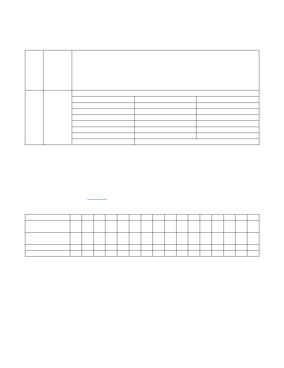
6.2.4.2ADCDataBuffer(ADDATAwhenADCFG=0)
When ADCFG = 0, reading from the ADDATA register reads the ADC results stored in one of the 16 data buffers . The
data buffer to read from is selected with the ADIDX[3:0] bits . Reading this register returns the 13-bit (12-bits plus a sign
bit) ADC conversion data plus selected data buffer memory . The ADIDX[3:0] bits automatically increment after a read of
ADDATA . This allows multiple reads of ADDATA to access consecutive data buffer locations without needing to change
ADIDX . The data buffers are reset to 0 on all forms of reset and are not writable by the user .
The data that is read from the ADC buffer can be from either a temperature or voltage conversion . Also, the data can
be right-aligned or left-aligned .
shows the returned bit weighting for each type of conversion .
Table6-3.ADCDataBitWeighting
3
ADDIFF
ADC Differential Mode Select . In voltage mode, this bit selects the ADC conversion mode . When
this bit is set to 1, the ADC conversion is in differential mode . When this bit is cleared to 0, the ADC
conversion is performed in single-ended mode . During single-ended mode, the sample is measured
between AD0P–AD5P and ground . If AD0P–AD5P transitions below 0, negative numbers are reported .
No clamping of data is performed for negative inputs . The firmware needs to clamp the negative read-
ing . In temperature mode, ADDIFF is a “don’t care .” The part automatically selects differential mode
for temperature measurement .
2:0
ADCH[2:0]
ADC Channel Select . These bits select the input channel source for the current ADC conversion .
ADCH[2:0]
ADDIFF=0
ADDIFF=1
000
AD0P
AD0P–AD0N
001
AD1P
AD1P–AD1N
010
AD2P
AD2P–AD2N
011
AD3P
AD3P–AD3N
100
AD4P
AD4P–AD4N
101
AD5P
AD5P–AD5N
11X
Internal Temperature Mode
Bit
15
14
13
12
11
10
9
8
7
6
5
4
3
2
1
0
Temperature Right-
Aligned
S
S
S
S
2
8
2
7
2
6
2
5
2
4
2
3
2
2
2
1
2
0
2
-1
2
-2
2
-3
Temperature Left-
Aligned
S
2
8
2
7
2
6
2
5
2
4
2
3
2
2
2
1
2
0
2
-1
2
-2
2
-3
0
0
0
Voltage Right-Aligned
S
S
S
S
2
11
2
10
2
9
2
8
2
7
2
6
2
5
2
4
2
3
2
2
2
1
2
0
Voltage Left-Aligned
S
2
11
2
10
2
9
2
8
2
7
2
6
2
5
2
4
2
3
2
2
2
1
2
0
0
0
0