5 pwm output mode, 12 .1 .5 pwm output mode -7, Table 12-3 . pwm output modes -7 – Maxim Integrated MAX31782 User Manual
Page 109: Figure 12-5 . pwm output mode block diagram -7, 5pwmoutputmode, Table12-3.pwmoutputmodes
MaximIntegrated 12-7
MAX31782 User’s Guide
Revision 0; 8/11
Figure 12-5. PWM Output Mode Block Diagram
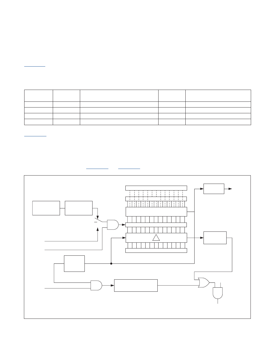
12.1.5PWMOutputMode
The PWM output mode is enabled when the Timer B is enabled (TRB = 1) and either the TBCS or TBCR bit is set to 1 .
describes how these bits determine the specific PWM operation . When operating as a PWM output, the
Timer B can provide up to 16-bit resolution of the PWM frequency or duty cycle . The counter in the Timer B can operate
as count up only, or count up/down .
shows a block diagram of the Timer B module when it is operating in PWM output mode . The TBB input
function (EXENB = 1) and the PWM/output control function (TBCS or TBCR
≠ 0) can be enabled at the same time . In
this configuration, the detection of a falling edge on the TBB pin results in the setting of the EXFB interrupt flag, but
does not force an auto-reload .
A timed setting or clearing of the TBB pin can also be generated without the need for the CPU to time the event or use
GPIO . This is accomplished by setting the compare register (TB0C) to a value greater than the reload register (TB0R) .
This functionality is illustrated in
.
Table12-3.PWMOutputModes
TBCS:TBCR
PWMMODE
TBBPINFUNCTION
INITIAL
STATE
NOTES
00
None
None (Disabled)
No change
01
Reset
Reset on TB0C Match, Set on 0000h
Low
Will not output a 0% duty cycle .
10
Set
Set on TB0C Match, Reset on TB0R Match
High
Will not output a 100% duty cycle .
11
Toggle
Toggle on TB0C Match
No change
SYSTEM
CLOCK
CLOCK PRESCALER
TBPS[2:0]
CLK
RELOAD
TBA PIN
TRB
EXENB
FALLING
EDGE
15
0
15
0
COMPARE
TB0V
0000h
EXFB = 1
TFB = 1
ETB
TIMER B
INTERRUPT
0
1
C/TB
TB0R
TB0C
TBCS
TBCR
TBB PIN