3 single step operation (trace), 17 .2 .3 single step operation (trace) -11, Table 17-4 – Maxim Integrated MAX31782 User Manual
Page 146: Maximintegrated 17-11
MaximIntegrated 17-11
MAX31782 User’s Guide
Revision 0; 8/11
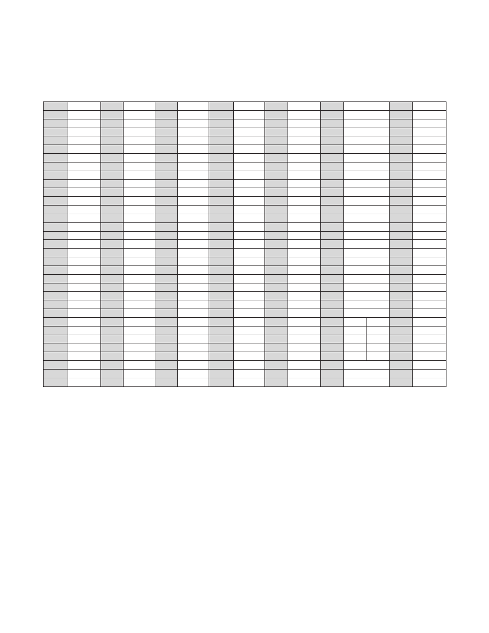
Table17-4.OutputfromReadRegisterMapCommand
17.2.3SingleStepOperation(Trace)
The debug engine supports single step operation in debug mode by executing a Trace command from the host . The
debug engine allows the CPU to return to its normal program execution for one cycle and then forces a debug mode
re-entry . The steps for the Trace command are:
1) Set status to 10b (debug-busy)
2) Pop the return address from the stack
3) Set the IGE bit to logic 1 if debug mode was activated when IGE = 1 .
4) Supply the CPU with an instruction addressed by the return address
5) Stall the CPU at the end of the instruction execution
6) Block the next instruction fetch from program memory
7) Push the return address onto the stack
8) Set the contents of IP to x8010h
9) Clear the IGE bit to 0 to disable the interrupt handler
10) Halt CPU operation
11) Set the status to debug-idle
WORD
REGISTER
WORD
REGISTER
WORD
REGISTER
WORD
REGISTER
WORD
REGISTER
WORD
REGISTER
WORD
REGISTER
0
PO2
32
----
64
----
96
PWMC0
128
PWMC2
160
MCNT
192
A[3]
1
PO1
33
I2CST_M
65
I2CST_S
97
PWMR0
129
PWMR2
161
MA
193
A[4]
2
----
34
I2CIE_M
66
I2CIE_S
98
PWMC1
130
PWMC3
162
MB
194
A[5]
3
MIIR0
35
PO6
67
MIIR2
99
PWMR1
131
PWMR3
163
MC2
195
A6[]
4
----
36
MIIR1
68
----
100
SMBUS
132
----
164
MC1
196
A[7]
5
----
37
----
69
----
101
TACHR0
133
TACHR2
165
MC0
197
A[8]
6
TB0C
38
EIF6
70
ADST
102
----
134
----
166
MC1R
198
A[9]
7
TB0R
39
EIE6
71
ADADDR
103
TACHR1
135
TACHR3
167
MC0R
199
A[10]
8
PI2
40
PI6
72
ADCN
104
PWMV0
136
PWMV2
168
PWMV4
200
A[11]
9
PI1
41
SVM
73
----
105
PWMCN0
137
PWMCN2
169
PWMCN4
201
A[12]
10
----
42
----
74
----
106
PWMV1
138
PWMV3
170
PWMC4
202
A[13]
11
TB0V
43
----
75
----
107
PWMCN1
139
PWMCN3
171
PWMR4
203
A[14]
12
----
44
I2CCN_M
76
I2CCN_S
108
TACHV0
140
TACHV2
172
TACHV4
204
A[15]
13
TB0CN
45
I2CCK_M
77
I2CCK_S
109
TACHCN0
141
TACHCN2
173
TACHCN4
205
IP
14
----
46
I2CTO_M
78
I2CTO_S
110
TACHV1
142
TACHV3
174
----
206
SP
15
----
47
I2CSLA_M
79
I2CSLA_S
111
TACHCN1
143
TACHCN3
175
TACHR4
207
IV
16
PD2
48
EIES6
80
----
112
MIIR3
144
MIIR4
176
----
208
LC[0]
17
PD1
49
----
81
----
113
----
145
----
177
TACHR5
209
LC[1]
18
----
50
PD6
82
----
114
----
146
----
178
TACHV5
210
OFFS
19
----
51
----
83
----
115
----
147
----
179
TACHCN5
211
DPC
20
----
52
----
84
----
116
----
148
----
180
PWMC5
212
GR
21
----
53
----
85
I2C_SPB
117
----
149
----
181
PWMR5
213
BP
22
----
54
ETS
86
DEV_NUM
118
----
150
----
182
PWMV5
214
DP[0]
23
----
55
ADCG1
87
----
119
----
151
----
183
PWMCN5
215
DP[1]
24
----
56
ADCG5
88
ICDT0
120
----
152
----
184
AP
APC
25
----
57
ADVOFF
89
ICDT1
121
----
153
----
185
PSF
IC
26
----
58
TOEX
90
ICDC
122
----
154
----
186
IMR
SC
27
----
59
----
91
ICDF
123
----
155
----
187
IIR
CKCN
28
----
60
----
92
ICDB
124
----
156
----
188
WDCN
00h
29
----
61
----
93
ICDA
125
----
157
----
189
A[0]
30
----
62
----
94
ICDD
126
----
158
----
190
A[1]
31
----
63
----
95
----
127
----
159
----
191
A[2]