1 detailed description, 1 pwm pin mapping and gpio muliplexing, 2 pwm operation – Maxim Integrated MAX31782 User Manual
Page 84: 9 .1 detailed description -3, 1detaileddescription, 1pwmpinmappingandgpiomuliplexing, 2pwmoperation
MaximIntegrated 9-3
MAX31782 User’s Guide
Revision 0; 8/11
9.1DetailedDescription
9.1.1PWMPinMappingandGPIOMuliplexing
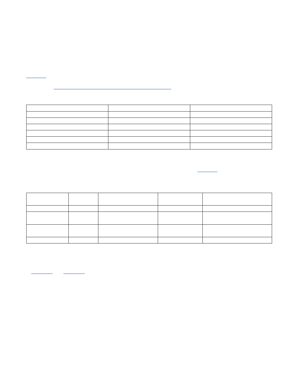
shows the mapping of each PWM Output . This table also shows that the PWM pins are mapped to GPIO
port P1[5:0] . When a PWM output pin’s functionality is disabled (PWMCS = 0 or PWMCR = 0), the pin can be used as
a GPIO . See
SECTION 11: General-Purpose Input/Output (GPIO) Pins
for information on using the PWM pins as GPIO .
9.1.2PWMOperation
A PWM output pin is enabled when either the PWMCS or PWMCR bit is set to 1 .
determine the specific PWM operation . The PWM counter does not begin operating until the PWMEN bit is set to 1 .
Table9-1.PWM/GPIOPinMultiplexing
Table9-2.PWMOutputModes
The PWM can provide up to 16-bit resolution of the frequency or duty cycle . A timed setting or clearing of the PWM .n pin
can also be generated without the need for the MAX31782 to time the event or use GPIO . This is accomplished by set-
ting the compare register (PWMCn) to a value greater than the reload register (PWMRn) . This functionality is illustrated
in
and
. The PWM can operate in a normal up-count-only configuration (DCEN = 0), or in a count
up/down configuration (DCEN = 1) .
PWMOUTPUTPIN
MAX31782PINNUMBER
GPIOPIN
PWM .0
28
P1 .0
PWM .1
26
P1 .1
PWM .2
24
P1 .2
PWM .3
20
P1 .3
PWM .4
18
P1 .4
PWM .5
16
P1 .5
PWMCS:PWMCR
PWMMODE
TBBPINFUNCTION
INITIALSTATE
WHENPWMEN=0
NOTES
00
None
None (Disabled)
No change
01
Reset
Reset on PWMCn Match
Set on 0000h
Low
Will not output a 0% duty cycle .
10
Set
Set on PWMCn Match
Reset on PWMRn Match
High
Will not output a 100% duty cycle
11
Toggle
Toggle on PWMCn Match
No change