5 interrupt mask register (imr, 8h[6h]), 6 system control register (sc, 8h[8h]), 5interruptmaskregister(imr,8h[6h]) – Maxim Integrated MAX31782 User Manual
Page 24: 6systemcontrolregister(sc,8h[8h])
3-6
MAX31782 User’s Guide
Revision 0; 8/11
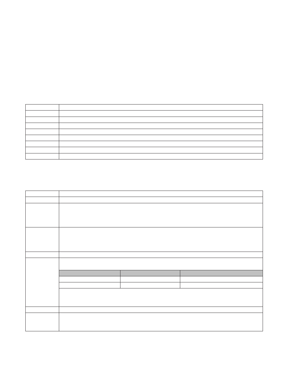
3.1.5InterruptMaskRegister(IMR,8h[6h])
Initialization: This register is cleared to 00h on all forms of reset .
Access: Unrestricted read/write access .
3.1.6SystemControlRegister(SC,8h[8h])
Initialization: This register is reset to 100000s0b on all reset . Bit 1 (PWL) is set to 1 on a power-on reset only .
Access: Unrestricted read/write access .
The first six bits in this register are interrupt mask bits for modules 0 to 5, one bit per module . The eighth bit, IMS, serves as a
mask for any system module interrupt sources . Setting a mask bit allows the enabled interrupt sources for the associated module
or system (for the case of IMS) to generate interrupt requests . Clearing the mask bit effectively disables all interrupt sources asso-
ciated with that specific module or all system interrupt sources (for the case of IMS) . The interrupt mask register is intended to
facilitate user-definable interrupt prioritization .
BIT
FUNCTION
IMR .0 (IM0)
Interrupt Mask for Register Module 0
IMR .1 (IM1)
Interrupt Mask for Register Module 1
IMR .2 (IM2)
Interrupt Mask for Register Module 2
IMR .3 (IM3)
Interrupt Mask for Register Module 3
IMR .4 (IM4)
Interrupt Mask for Register Module 4
IMR .5 (IM5)
Interrupt Mask for Register Module 5
IMR .6
Reserved . Reads return 0 .
IMR .7 (IMS)
Interrupt Mask for System Modules
BIT
FUNCTION
SC .0
Reserved . All reads return 0 .
SC .1 (PWL)
Password Lock . This bit defaults to 1 on a power-on reset . When this bit is 1, it requires a 32-byte password to
be matched with the password in the program space before allowing access to the ROM loader’s utilities for
read/write of program memory and debug functions . Clearing this bit to 0 disables the password protection to
the ROM loader .
SC .2 (ROD)
ROM Operation Done . This bit is used to signify completion of a ROM operation sequence to the control units .
This allows the debug engine to determine the status of a ROM sequence . Setting this bit to logic 1 causes an
internal system reset if the JTAG_SPE bit is also set . Setting the ROD bit clears the JTAG_SPE bit if it is set and
the ROD bit is automatically cleared by hardware once the control unit acknowledges the done indication .
SC .3
Reserved . All reads return 0 .
SC .4 (CDA0)
Code Data Access Bit 0 . The CDA bit is used to logically map physical program memory page to the data
space for read/write access:
CDA0
BYTE MODE ACTIVE PAGE
WORD MODE ACTIVE PAGE
0
P0
P0 and P1
1
P1
P0 and P1
The logical addresses depend on which memory segment is executing . Note that CDA1 (normally at bit posi-
tion SC .5) is not implemented since the maximum flash memory size is 64KB or 32KWords .
SC .[6:5]
Reserved . All reads return 0 .
SC .7 (TAP)
Test Access (JTAG) Port Enable . This bit controls whether the test access port special-function pins are
enabled . The TAP defaults to being enabled . Clearing this bit to 0 disables the TAP special-function pins on the
JTAG pins .