18 data pointer control register (dpc, eh[4h]), 19 general register (gr, eh[5h]), 20 general register low byte (grl, eh[6h]) – Maxim Integrated MAX31782 User Manual
Page 29: 18datapointercontrolregister(dpc,eh[4h]), 19generalregister(gr,eh[5h]), 20generalregisterlowbyte(grl,eh[6h])
MaximIntegrated 3-11
MAX31782 User’s Guide
Revision 0; 8/11
3.1.18DataPointerControlRegister(DPC,Eh[4h])
Initialization: This register is cleared to 001Ch on all forms of reset .
Access: Unrestricted direct read/write access .
3.1.19GeneralRegister(GR,Eh[5h])
Initialization: This register is cleared to 0000h on all forms of reset .
Access: Unrestricted direct read/write access .
3.1.20GeneralRegisterLowByte(GRL,Eh[6h])
Initialization: This register is cleared to 00h on all forms of reset .
Access: Unrestricted direct read/write access .
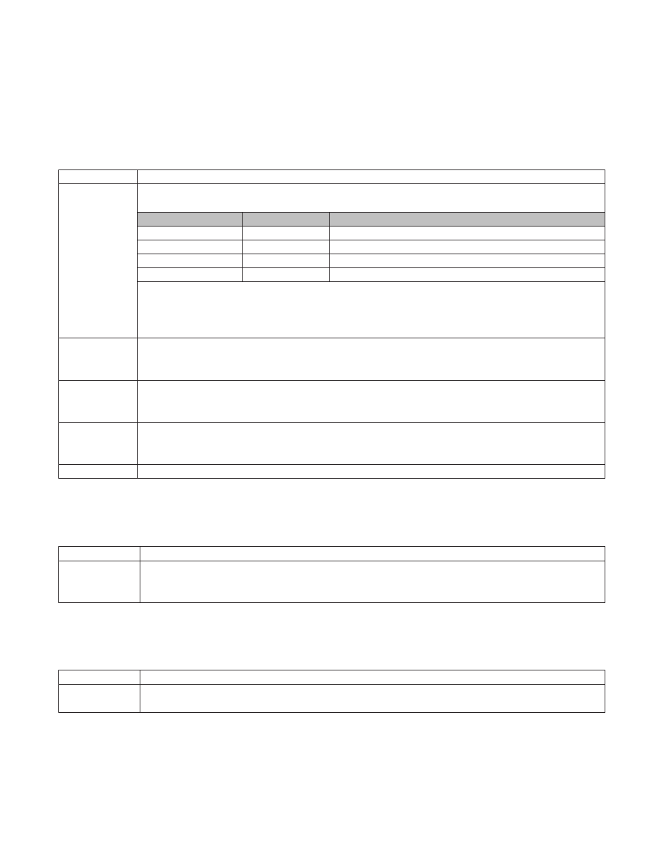
BIT
FUNCTION
DPC .[1:0]
(SDPS[1:0])
Source Data Pointer Select Bits 1:0 . These bits select one of the three data pointers as the active source point-
er for the load operation . A new data pointer must be selected before being used to read data memory:
SDPS1
SDPS0
SOURCE POINTER SELECTION
0
0
DP[0]
0
1
DP[1]
1
0
FP (BP[OFFS])
1
1
Reserved (select FP if set)
These bits default to 00b but do not activate DP[0] as an active source pointer until the SDPS bits are explicitly
cleared to 00b or the DP[0] register is written by an instruction . Also, modifying the register contents of a data/
frame pointer register (DP[0], DP[1], BP, or OFFS) changes the setting of the SDPS bits to reflect the active
source pointer selection .
DPC .2 (WBS0)
Word/Byte Select 0 . This bit selects access mode for DP[0] . When WBS0 is set to logic 1, the DP[0] is oper-
ated in word mode for data memory access; when WBS0 is cleared to logic 0, DP[0] is operated in byte mode
for data memory access .
DPC .3 (WBS1)
Word/Byte Select 1 . This bit selects access mode for DP[1] . When WBS1 is set to logic 1, the DP[1] is oper-
ated in word mode for data memory access; when WBS1 is cleared to logic 0, DP[1] is operated in byte mode
for data memory access .
DPC .4 (WBS2)
Word/Byte Select 2 . This bit selects access mode for BP[OFFS] . When WBS2 is set to logic 1, the BP[OFFS]
is operated in word mode for data memory access; when WBS2 is cleared to logic 0, BP[OFFS] is operated in
byte mode for data memory access .
DPC .[15:5]
Reserved . Read returns 0 .
BIT
FUNCTION
GR .[15:0]
This register is intended primarily for supporting byte operations on 16-bit data . The 16-bit register is byte-
readable, byte-writable through the corresponding GRL and GRH 8-bit registers and byte-swappable through
the GRS 16-bit register .
BIT
FUNCTION
GRL .[7:0]
This register reflects the low byte of the GR register and is intended primarily for supporting byte operations
on 16-bit data . Any data written to the GRL register is also stored in the low byte of the GR register .