2 adc status register (adst), 3 adc address register (adaddr), 2adcstatusregister(adst) – Maxim Integrated MAX31782 User Manual
Page 50: 3adcaddressregister(adaddr), Register address: m2[06h, Register address: m2[07h
MaximIntegrated 6-7
MAX31782 User’s Guide
Revision 0; 8/11
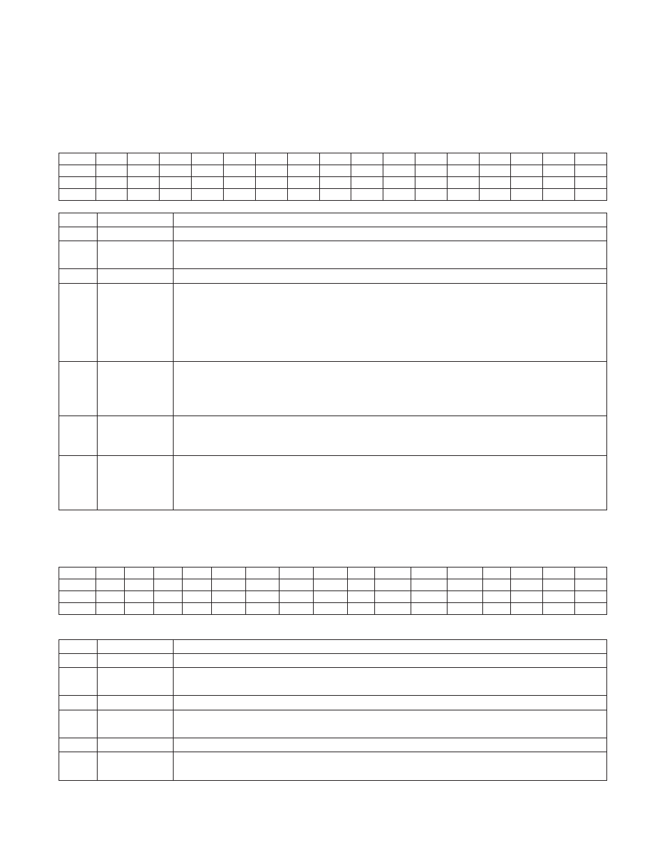
6.2.2ADCStatusRegister(ADST)
Register Address: M2[06h]
6.2.3ADCAddressRegister(ADADDR)
Register Address: M2[07h]
*Unrestricted read, but can only be written to when ADCONV = 0.
Bit
15
14
13
12
11
10
9
8
7
6
5
4
3
2
1
0
Name
—
—
—
—
ADDAT3 ADDAT2 ADDAT1 ADDAT0
—
ADCONV
ADDAI
ADCFG
ADIDX3
ADIDX2
ADIDX1
ADIDX0
Reset
0
0
0
0
0
0
0
0
0
0
0
0
0
0
0
0
Access
r
r
r
r
r
r
r
r
r
rw
rw
rw
rw
rw
rw
rw
BIT
NAME
DESCRIPTION
15:12
—
Reserved . The user should not write to these bits .
11:8
ADDAT[3:0]
ADC Data Available Address Bits [3:0] . These bits indicate the memory location last written to by the
ADC . These bits are read-only .
7
—
Reserved . The user should not write to this bit .
6
ADCONV
ADC Start Conversion . Set this bit to 1 start the conversion process . This bit remains set until the
conversion process is finished . In single sequence mode, this bit is cleared to 0 when the conversion
sequence is finished . In continuous sequence mode, this bit remains set until the ADC conversion is
stopped . To stop ADC conversion at any time, write 0 to this bit . The ADC stops acquiring data after
the current conversion is finished, or, if the ADC is waiting during extended acquisition time, the ADC
stops immediately . This bit is cleared to 0 on entry of stop mode .
5
ADDAI
ADC Data Available Interrupt Flag . This bit is set to 1 when the condition matching ADDAINV bits
are met . The ADC memory location last written by the ADC is available at ADDAT . This flag causes
an interrupt if the ADDAIE is enabled . This bit is cleared by software writing a 0 or when software
changes ADCONV bit from 0 to 1 .
4
ADCFG
ADC Conversion Configuration Register Select . This bit selects the target register pointed to by ADIDX .
When ADCFG is set to 1, the ADIDX[2:0] configuration register is selected for read/write access . When
ADCFG is cleared to 0, the ADIDX[3:0] data buffer location is selected for reading only .
3:0
ADIDX[3:0]
ADC Register Index Bits [3:0] . These bits together with ADCFG select the source/destination for
ADDATA access . When ADCFG = 0, ADIDX[3:0] are used to address one of the 16 data buffers .
When ADCFG = 1, only ADIDX[2:0] are used to address one of the eight configuration registers . This
register value is auto-incremented on successive access (read/write) of ADDATA register .
Bit
15
14
13
12
11
10
9
8
7
6
5
4
3
2
1
0
Name
—
—
—
—
ADBADD3 ADBADD2 ADBADD1 ADBADD0
—
ADSTART2 ADSTART1 ADSTART0
—
ADEND2 ADEND1 ADEND0
Reset
0
0
0
0
0
0
0
0
0
0
0
0
0
0
0
0
Access
r
r
r
r
rw*
rw*
rw*
rw*
r
rw*
rw*
rw*
r
rw*
rw*
rw*
BIT
NAME
DESCRIPTION
15:12
—
Reserved . The user should not write to these bits .
11:8
ADBADD[3:0]
ADC Data Buffer Address Bits [3:0] . These bits indicate the first ADC acquisition data memory loca-
tion . These bits can be written to only when ADCONV = 0 .
7
—
Reserved . The user should not write to this bit .
6:4
ADSTART[2:0]
ADC Conversion Configuration Start Address Bits [2:0] . These bits select the first conversion configu-
ration register .
3
—
Reserved . The user should not write to this bit .
2:0
ADEND[2:0]
ADC Conversion Configuration Ending Address Bits [2:0] . These bits select the last conversion con-
figuration register . This register is inclusive when defining the sequence .