4 i2c slave address register (i2csla_s), 5 i2c slave data buffer register (i2cbuf_s), 7 .2 .4 i – Maxim Integrated MAX31782 User Manual
Page 67: C slave address register (i2csla_s) -11, 7 .2 .5 i, C slave data buffer register (i2cbuf_s) -11, Cslaveaddressregister(i2csla�s), Cslavedatabufferregister(i2cbuf�s), Address: m2[0fh, Address: m2[00h
MaximIntegrated 7-11
MAX31782 User’s Guide
Revision 0; 8/11
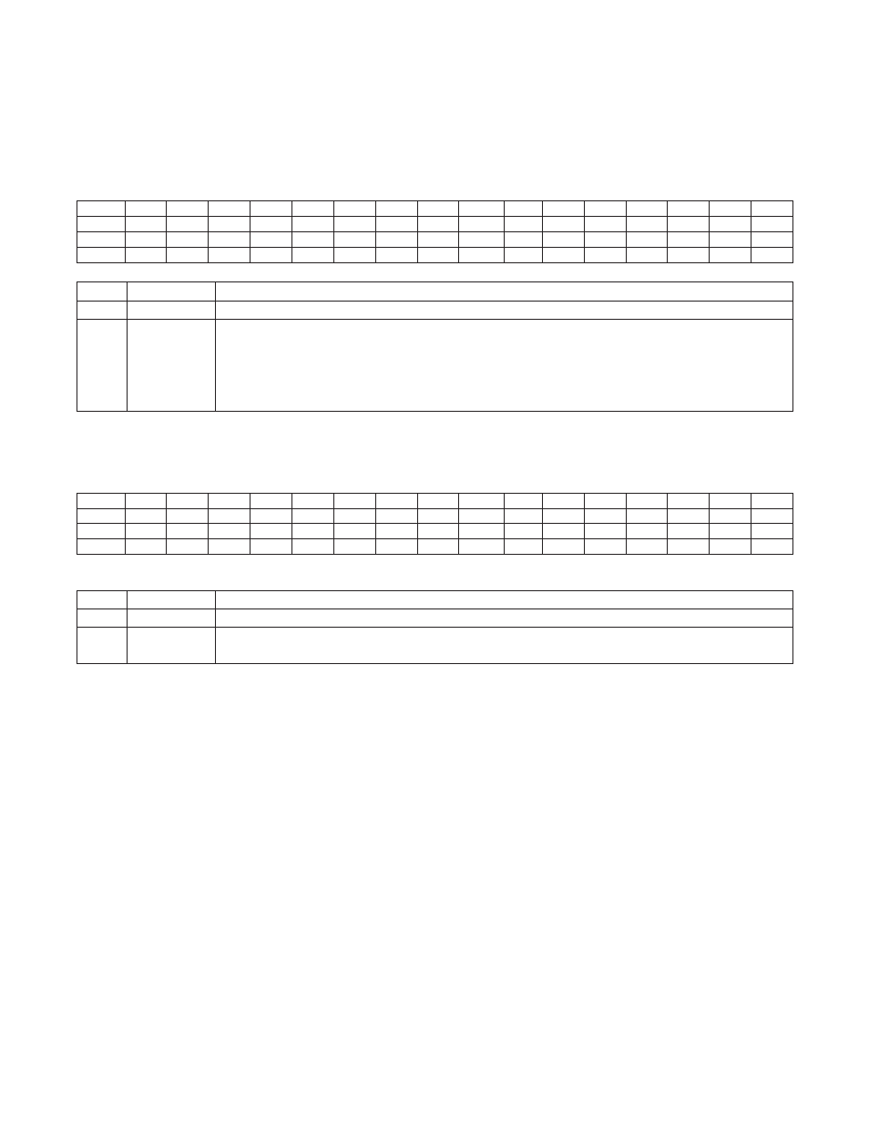
7.2.4I
2
CSlaveAddressRegister(I2CSLA�S)
Address: M2[0Fh]
7.2.5I
2
CSlaveDataBufferRegister(I2CBUF�S)
Address: M2[00h]
*Unrestricted read access. This register can be written to only when I2CBUSY = 0.
Bit
15
14
13
12
11
10
9
8
7
6
5
4
3
2
1
0
Name
—
—
—
—
—
—
—
—
—
A6
A5
A4
A3
A2
A1
A0
Reset
0
0
0
0
0
0
0
0
0
0
0
1
1
0
1
1
Access
r
r
r
R
r
r
r
r
r
rw
rw
rw
rw
rw
rw
rw
BIT
NAME
DESCRIPTION
15:7
—
Reserved . The user should not write to these bits .
6:0
A[6:0]
These address bits contain the address of the I
2
C slave interface . When a match to this address is
detected, the I
2
C controller automatically acknowledges the host with the I2CACK bit value and the
I2CAMI flag is set to 1 . An interrupt is generated if enabled . The address in I2CSLA is the device slave
address without the R/W bit . For example, the default value of I2CSLA_S is 1Bh, which produces a
device slave address of 36h .
Bit
15
14
13
12
11
10
9
8
7
6
5
4
3
2
1
0
Name
—
—
—
—
—
—
—
—
D7
D6
D5
D4
D3
D2
D1
D0
Reset
0
0
0
0
0
0
0
0
0
0
0
0
0
0
0
0
Access
r
r
r
R
r
r
r
r
rw*
rw*
rw*
rw*
rw*
rw*
rw*
rw*
BIT
NAME
DESCRIPTION
15:8
—
Reserved . The user should not write to these bits .
7:0
D[7:0]
Data for I
2
C transfer is read from or written to this location . The I
2
C transmit and receive buffers are
separate, but both are addressed at this location .