Using the combined chip-enable signals, Sing the combined chip, Enable signals – Maxim Integrated High-Speed Microcontroller Users Guide: DS80C390 Supplement User Manual
Page 94
High-Speed Microcontroller User’s Guide: DS80C390 Supplement
94 of 158
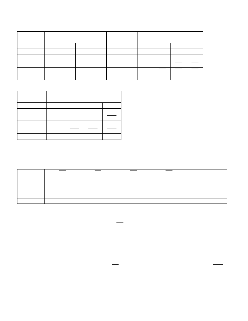
Table 6-2. EXTENDED ADDRESS AND CHIP ENABLE GENERATION
Port 4 Pin Function
(A19-A16 Address Pins)
Port 4 Pin Function
(Code Memory Chip Enables)
P4CNT.5-3 P4.7 P4.6 P4.5 P4.4 P4CNT.2-0 P4.3 P4.2 P4.1 P4.0
000 I/O I/O I/O I/O
000
I/O I/O I/O I/O
100 I/O I/O I/O A16
100
I/O I/O I/O
CE0
101 I/O
I/O
A17
A16 101 I/O
I/O
CE1
CE0
110 I/O
A18
A17
A16 110 I/O
CE2
CE1
CE0
111(default) A19 A18 A17 A16 111(default)
CE3
CE2
CE1
CE0
Port 5 Pin Function
(MOVX Memory Chip Enables)
P5CNT.2-0 P5.7 P5.6 P5.5 P5.4
000(default)
I/O I/O I/O I/O
100 I/O I/O I/O
PCE0
101 I/O
I/O
PCE1
PCE0
110 I/O
PCE2
PCE1
PCE0
111
PCE3
PCE2
PCE1
PCE0
The following table illustrates how memory is segmented based on the setting of the Port 4 P4.7-4
Configuration Control bits (P4CNT.5-3).
Table 6-3. PROGRAM MEMORY CHIP-ENABLE BOUNDARIES
P4CNT.5-3
CE0
CE1
CE2
CE3
Maximum Memory
size per Chip Enable
000 0h-7FFFh
8000h-FFFFh
10000h-17FFFh 18000h-1FFFFh
32
kilobytes
100 0h-1FFFFh
20000h-3FFFFh
40000h-5FFFFh 60000h-7FFFFh
128
kilobytes
101 0h-3FFFFh
40000h-7FFFFh 80000h-BFFFFh C0000h-FFFFFh 256
kilobytes
110 0h-7FFFFh
80000h-FFFFFh
100000h-17FFFFh
180000h-1FFFFFh
512
kilobytes
111(default) 0-FFFFFh 100000h-1FFFFFh
200000h-2FFFFFh
300000h-3FFFFFh 1
megabyte
Following any reset, the device defaults to 16-bit mode addressing. In 16-bit addressing mode the device
will be configured with P4.7-P4.4 as address lines and P4.3-P4.0 configured as
0
-
CE3
, with the first
program fetch being performed from 00000h with
CE0
active (low).
USING THE COMBINED CHIP-ENABLE SIGNALS
The DS80C390 incorporates a feature allowing
PCEx
and
CEx
signals to be combined. This is useful
when incorporating modifiable code memory as part of a bootstrap loader or for in-system
reprogrammability. Setting the one or more
0
PDCE3
−
bits (MCON.3-0) causes the corresponding chip
enable signal to be asserted for both MOVC and MOVX operations. Write access to combined program
and data memory blocks is controlled by the
WR
signal, and read access is controlled by the
PSEN
signal. This feature is especially useful if the design achieves in-system reprogrammability by external
Flash memory, in which a single device is accessed by both MOVC instructions (program fetch) and
MOVX write operations (updates to code memory).