Addendum to section 6: memory access, External memory interfacing – Maxim Integrated High-Speed Microcontroller Users Guide: DS80C390 Supplement User Manual
Page 93
High-Speed Microcontroller User’s Guide: DS80C390 Supplement
93 of 158
ADDENDUM TO SECTION 6: MEMORY ACCESS
EXTERNAL MEMORY INTERFACING
The DS80C390 follows the memory interface convention established by the industry standard
80C32/80C52, but with many added improvements. Most notably, the device incorporates a 22-bit
addressing capability that supports up to four megabytes of program memory and four megabytes of data
memory. Externally the memory is accessed by a multiplexed or demultiplexed 20-bit address bus/8-bit
data bus and four chip enable (active during program memory access) or four peripheral enable (active
during data memory access) signals. Multiplexed addressing mode mimics the traditional 8051 memory
interface, with the address MSB presented on Port 2 and the address LSB and data multiplexed on Port 0.
The multiplexed mode requires an external latch to demultiplex the address LSB and data. When the
MUX pin is pulled high, the address LSB and data are demultiplexed, with the address MSB presented on
Port 2, address LSB on Port 1, and the data on Port 0. The elimination of the demultiplexing latch
removes a delay element in the memory timing, and can in some cases allow the use of slower, less
expensive memory devices. The following table illustrates the locations of the external memory control
signals.
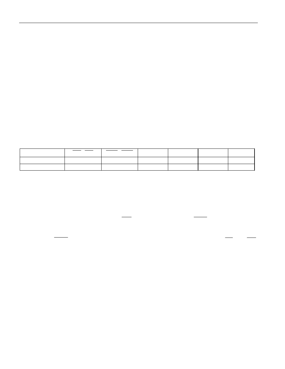
Table 6-1. EXTERNAL MEMORY ADDRESSING PIN ASSIGNMENTS
Address/Data Bus
CE3
-
CE0
PCE3
-
PCE0
Addr 19-16 Addr 15-8
Addr 7-0 Data Bus
Multiplexed P4.3-P4.0 P5.7-P5.4
P4.7-P4.4 P2
P0
P0
Demultiplexed P4.3-P4.0 P5.7-P5.4 P4.7-P4.4 P2
P1
P0
Each upper order address line (A16-A19) and chip or peripheral enable is individually enabled by the
P4CNT and P5CNT registers. Enabling upper order address lines controls the maximum size of the
external memories that can be addressed, and enabling chip or peripheral enables controls the number of
external memories that can be addressed. For example, if P4CNT.5-3 are set to 101b, A17 and A16 will
be enabled (along with A15-0), permitting a maximum memory device size of 2
18
or 256 KB.
The configurable program/code chip enable ( CEx ) and MOVX chip-enable ( PCEx ) signals issued by the
microprocessor are used when accessing multiple external memory devices. External chip enable lines are
only required if more than one physical block of memory will be used. In the standard 8051
configuration, PSEN is used as the output enable for the program memory device, and RD and WR
control the input or output functions of the data (SRAM) device. The chip enables of these devices can be
connected to their active state if only one of each will be used. To support a larger amount of memory,
however, the microprocessor must generate chip or data enables to select one of several memory devices.
The following tables demonstrate how to enable various combinations of high-order address lines and
chip enables.