Can standard global mask register 0 (cnsgm0), Can standard global mask register 1 (cnsgm1) – Maxim Integrated High-Speed Microcontroller Users Guide: DS80C390 Supplement User Manual
Page 127
High-Speed Microcontroller User’s Guide: DS80C390 Supplement
127 of 158
TSEG13 TSEG12 TSEG11 TSEG10 Time Segment One Length
(Number in parenthesis is TS1_LEN
value used in bit timing calculations)
0 0 0 0
Invalid
0 0 0 1
2
t
qu
(2)
0 0 1 0
3
t
qu
(3)
. . . .
.
1 1 1 0
15
t
qu
(15)
1 1 1 1
16
t
qu
(16)
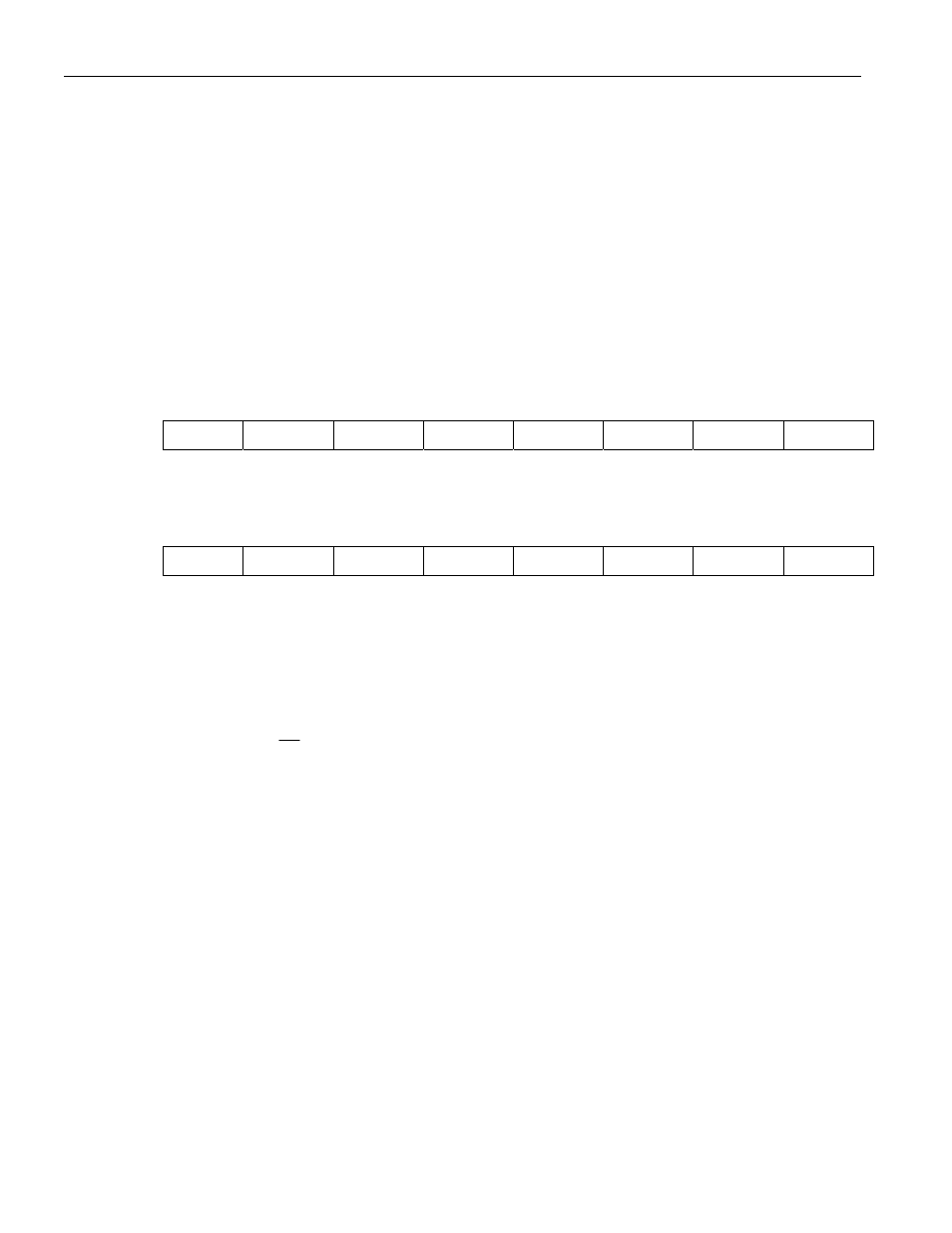
CAN Standard Global Mask Register 0 (CnSGM0)
MOVX
Address
1
7
6
5
4
3
2
1
0
xxxx06h MASK28 MASK27 MASK26 MASK25 MASK24 MASK23 MASK22 MASK21
CAN Standard Global Mask Register 1 (CnSGM1)
MOVX
Address
1
7
6
5
4
3
2
1
0
xxxx07h
MASK20
MASK19
MASK18
0 0 0 0 0
CAN Standard Global Mask Registers 1-0. These registers function as the
mask when performing the 11-bit global identification test on incoming messages
for Message Centers 1-14. If MEME=0, the incoming message ID field must
match the corresponding message center arbitration value exactly, effectively
ignoring the contents of these registers. These registers are only used when
performing the standard identification test, and their contents are ignored when
EX/ST =1. These registers can only be modified during a software initialization
(SWINT=1).
Any mask bit in the CnSGM1, CnSGM0 mask programmed to a 0 will create a
don’t care condition when the respective bit in the incoming message ID field is
compared with the corresponding arbitration bits in Message Centers 1-14. Any
bit in these masks programmed to a 1 will force the respective bit in the incoming
message ID field to match identically with the corresponding arbitration bits in
Message Centers 1-14, before said message will be loaded into Message Centers
1-14.
The five least significant bits in the CnSGM1 register are not used, and will not
perform any comparison of these bit locations. A read of these bits will return a 0,
writes are ignored..