Can 0 message center 15 control register (c0m15c), Serial port control (scon1), Can 0 m – Maxim Integrated High-Speed Microcontroller Users Guide: DS80C390 Supplement User Manual
Page 55: Essage, Enter, 15 c, Ontrol, Egister, C0m15c), Erial
High-Speed Microcontroller User’s Guide: DS80C390 Supplement
55 of 158
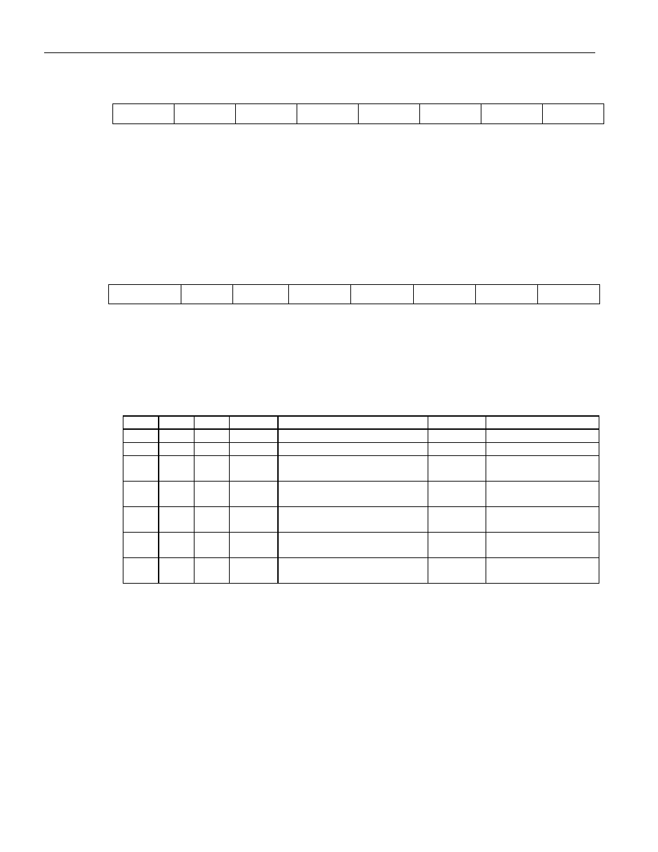
CAN 0 MESSAGE CENTER 15 CONTROL REGISTER (C0M15C)
7 6 5 4 3 2 1 0
SFR BFh
MSRDY
ETI
ERI
INTRQ
EXTRQ
MTRQ ROW/TIH
DTUP
RW-0 RW-0 RW-0 RW-0 RC-0 R*-0 R*-0 R*-0
R = Unrestricted Read, C = Clear Only, * = See description below, -n = Value after Reset
C0M15C
Bits 7-0
Operation of the bits in this register are identical to those found in the CAN 0
Message One Control Register (C0M1C;ABh). Please consult the description
of that register for more information.
SERIAL PORT CONTROL (SCON1)
7 6
5 4 3 2 1 0
SFR C0h SM0/FE_1 SM1_1 SM2_1
REN_1
TB8_1
RB8_1
TI_1
RI_1
RW-0 RW-0
RW-0 RW-0 RW-0 RW-0 RW-0 RW-0
R = Unrestricted Read, W = Unrestricted Write, -n = Value after Reset
SM0-2
Bits 7-5
Serial Port 1 Mode. These bits control the mode of serial port 1 as shown below.
In addition, the SM0 and SM2 bits have secondary functions as shown below.
SM0 SM1 SM2 MODE
FUNCTION LENGTH
PERIOD
0 0 0 0
Synchronous
8
bits
12
t
CLK
0 0 1 0
Synchronous
8
bits
4
t
CLK
0 1 X 1
Asynchronous
10
bits
Timer 1 or 2
baud rate equation
1 0 0 2
Asynchronous
11
bits 64 t
CLK
(SMOD=0)
32 t
CLK
(SMOD=1)
1 0 1 1
Asynchronous with
Multiprocessor communication
11 bits
64 t
CLK
(SMOD=0)
32 t
CLK
(SMOD=1)
1 1 0 3
Asynchronous
11
bits
Timer 1 or 2
baud rate equation
1 1 1 3
Asynchronous with
Multiprocessor communication
11 bits
Timer 1 or 2
baud rate equation
SM0/FE_1
Bit 7
Framing Error Flag. When SMOD0 (PCON.6)=0, this bit (SM0) is used to
select the mode for serial port 1. When SMOD0 (PCON.6)=1, this bit (FE) will
be set upon detection of an invalid stop bit. When used as FE, this bit must be
cleared in software. Once the SMOD0 bit is set, modifications to this bit will not
affect the serial port mode settings. Although accessed from the same register,
internally the data for bits SM0 and FE are stored in different locations.
SM1_1
Bit 6
No alternate function.
SM2-2
Bit 5
Multiple CPU Communications. The function of this bit is dependent on the
serial port 0 mode.
Mode 0: Selects 12 t
CLK
or 4 t
CLK
period for synchronous serial port 0 data
transfers.