Can 0 message center 4 control register (c0m4c), Can 0 message center 5 control register (c0m5c), Port 3 (p3) – Maxim Integrated High-Speed Microcontroller Users Guide: DS80C390 Supplement User Manual
Page 50: Can 0 m, Essage, Enter, Ontrol, Egister, C0m4c), C0m5c)
High-Speed Microcontroller User’s Guide: DS80C390 Supplement
50 of 158
CAN 0 MESSAGE CENTER 4 CONTROL REGISTER (C0M4C)
7 6 5 4 3 2 1 0
SFR AEh
MSRDY
ETI
ERI
INTRQ
EXTRQ
MTRQ ROW/TIH
DTUP
RW-0 RW-0 RW-0 RW-0 RC-0 R*-0 R*-0 R*-0
R = Unrestricted Read, C = Clear Only, * = See description below, -n = Value after Reset
C0M4C
Bits 7-0
Operation of the bits in this register are identical to those found in the CAN 0
Message One Control Register (C0M1C;ABh). Please consult the description
of that register for more information.
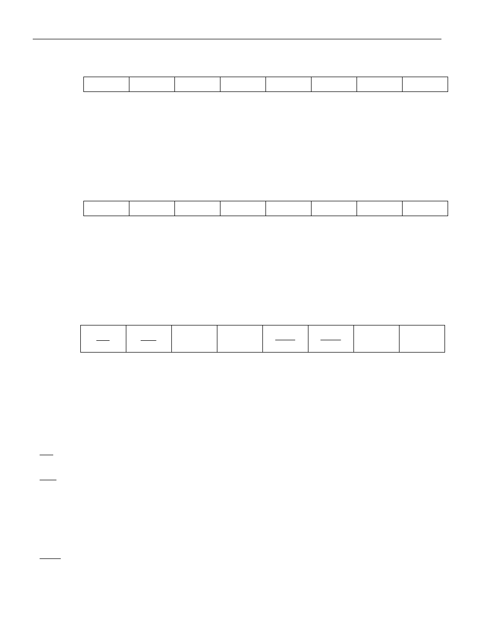
CAN 0 MESSAGE CENTER 5 CONTROL REGISTER (C0M5C)
7 6 5 4 3 2 1 0
SFR AFh
MSRDY
ETI
ERI
INTRQ
EXTRQ
MTRQ ROW/TIH
DTUP
RW-0 RW-0 RW-0 RW-0 RC-0 R*-0 R*-0 R*-0
R = Unrestricted Read, C = Clear Only, * = See description below, -n = Value after Reset
C0M5C
Bits 7-0
Operation of the bits in this register are identical to those found in the CAN 0
Message One Control Register (C0M1C;ABh). Please consult the description
of that register for more information.
PORT 3 (P3)
7 6 5 4 3 2 1 0
SFR B0h
P3.7
RD
P3.6
WR
P3.5
T1
P3.4
T0
P3.3
INT1
P3.2
INT0
P3.1
TXD0
P3.0
RXD0
RW-1 RW-1 RW-1 RW-1 RW-1 RW-1 RW-1 RW-1
R = Unrestricted Read, W = Unrestricted Write, -n = Value after Reset
P3.7-0
Bits 7-0
General-Purpose I/O Port 3. This register functions as a general-purpose I/O
port. In addition, all the pins have an alternative function listed below. Each of
the functions is controlled by several other SFRs. The associated Port 1 latch bit
must contain a logic one before the pin can be used in its alternate function
capacity.
RD
Bit 7
External Data Memory Read Strobe. This pin provides an active low read
strobe to an external memory device.
WR
Bit 6
External Data Memory Write Strobe. This pin provides an active low write
strobe to an external memory device.
T1
Bit 5
Timer/Counter External Input. A 1 to 0 transition on this pin will increment
Timer 1.
T0
Bit 4
Counter External Input. A 1 to 0 transition on this pin will increment Timer 0.
INT1
Bit 3
External Interrupt 1. A falling edge/low level on this pin will cause an external
interrupt 1 if enabled.