Hanging the, Ystem, Lock – Maxim Integrated High-Speed Microcontroller Users Guide: DS80C390 Supplement User Manual
Page 92: Achine, Ycle, Requency
High-Speed Microcontroller User’s Guide: DS80C390 Supplement
92 of 158
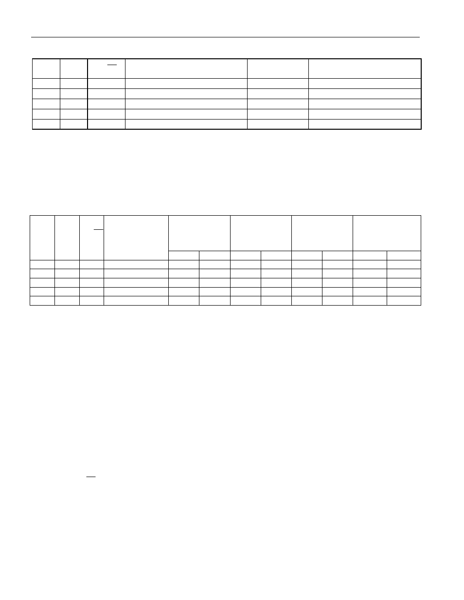
Table 5-1. SYSTEM CLOCK CONFIGURATION
CD1 CD0
2X
4X/
NAME CLOCKS/MC
MAX EXTERNAL
FREQUENCY (MHz)
0
0
0
Frequency Multiplier (2X)
2
20
0
0
1
Frequency Multiplier (4X)
1
10
0 1 N/A
Reserved
—
—
1 0 N/A
Divide-by-4
(Default)
4
40
1
1
N/A
Power Management Mode
1024
40
The system clock and machine cycle rate changes one machine cycle after the instruction changing the
control bits. Note that the change will affect all aspects of system operation, including timers and baud
rates. The use of the switchback feature, described later, can eliminate many of the issues associated with
the Power Management Mode’s effect on peripherals such as the serial port. Table 5-2 illustrates the
effect of the clock modes on the operation of the timers.
Table 5-2. EFFECT OF CLOCK MODES ON TIMER OPERATION
OSC. CYCLES
PER TIMER
0/1/2 CLOCK
OSC. CYCLES
PER TIMER 2
CLOCK, BAUD
RATE GEN.
OSC. CYCLES
PER SERIAL
PORT CLOCK
MODE 0
OSC. CYCLES
PER SERIAL
PORT CLOCK
MODE 2
CD1 CD0
2X
4X/
OSC. CYCLES
PER MACHINE
CYCLE
TxM=1 TxM=0 T2M=1 T2M=0 SM2=0 SM2=1 SMOD=0 SMOD=1
0
0
0
2
2 12 2 2 6 2 64 32
0
0
1
1
1 12 2 2 3 1 64 32
0
1
N/A
Reserved
1 0
N/A
4
4 12 2 2 12 4 64 32
1 1 N/A
1024
1024 3072 512 512 3072 1024 16,384 8192
CHANGING THE SYSTEM CLOCK/MACHINE CYCLE CLOCK FREQUENCY
The microcontroller incorporates a special locking sequence to ensure “glitch-free” switching of the
internal clock signals. All changes to the CD1, CD0 bits must pass through the 10 (divide-by-4) state.
For example, to change from 00 (frequency multiplier) to 11 (PMM), the software must change the bits in
the following sequence: 00
⇒ 10 ⇒ 11. Attempts to switch between invalid states will fail, leaving the
CD1, CD0 bits unchanged.
The following sequence must be followed when switching to the frequency multiplier as the internal time
source. This sequence can only be performed when the device is in divide-by-four operation. The steps
must be followed in this order, although it is possible to have other instructions between them. Any
deviation from this order will cause the CD1, CD0 bits to remain unchanged. Switching from frequency
multiplier to non-multiplier mode requires no steps other than the changing of the CD1, CD0 bits.
1. Ensure that the CD1, CD0 bits are set to 10, and the RGMD (EXIF.2) bit = 0.
2. Clear the CTM (Crystal Multiplier Enable) bit.
3. Set the
2X
4X/
bit to the appropriate state.
4. Set the CTM (Crystal Multiplier Enable) bit.
5. Poll the CKRDY bit (EXIF.3), waiting until it is set to 1. This will take approximately 65536 cycles
of the external crystal or clock source.
6. Set CD1, CD0 to 00. The frequency multiplier will be engaged on the machine cycle following the
write to these bits.