I/o-ports, Port a, The port a data register - porta – Rainbow Electronics ATmega163L User Manual
Page 99: The port a data direction register - ddra, The port a input pins address - pina, Port a as general digital i/o, Atmega163(l)
ATmega163(L)
99
I/O-Ports
All AVR ports have true Read-Modify-Write functionality when used as general digital I/O ports. This means that the direc-
tion of one port pin can be changed without unintentionally changing the direction of any other pin with the SBI and CBI
instructions. The same applies for changing drive value (if configured as output) or enabling/disabling of pull-up resistors (if
configured as input).
Port A
Port A is an 8-bit bi-directional I/O port with internal pull-ups.
Three I/O memory address locations are allocated for Port A, one each for the Data Register - PORTA, $1B($3B), Data
Direction Register - DDRA, $1A($3A) and the Port A Input Pins - PINA, $19($39). The Port A Input Pins address is read
only, while the Data Register and the Data Direction Register are read/write.
All port pins have individually selectable pull-up resistors. The PORT A output buffers can sink 20mA and thus drive LED
displays directly. When pins PA0 to PA7 are used as inputs and are externally pulled low, they will source current if the
internal pull-up resistors are activated.
Port A has an alternate function as analog inputs for the ADC. If some Port A pins are configured as outputs, it is essential
that these do not switch when a conversion is in progress. This might corrupt the result of the conversion.
During powerdown mode, the schmitt trigger of the digital input is disconnected. This allows analog signals that are close to
V
CC
/2 to be present during powerdown without causing excessive power consumption.
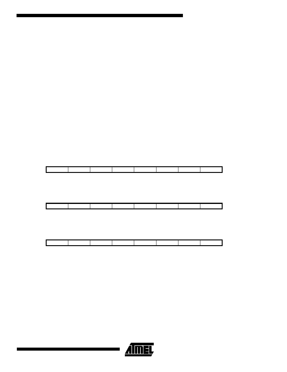
The Port A Data Register - PORTA
The Port A Data Direction Register - DDRA
The Port A Input Pins Address - PINA
The Port A Input Pins address - PINA - is not a register, and this address enables access to the physical value on each Port
A pin. When reading PORTA the PORTA Data Latch is read, and when reading PINA, the logical values present on the
pins are read.
PORT A as General Digital I/O
All 8 bits in PORT A are equal when used as digital I/O pins.
PAn, General I/O pin: The DDAn bit in the DDRA register selects the direction of this pin, if DDAn is set (one), PAn is con-
figured as an output pin. If DDAn is cleared (zero), PAn is configured as an input pin. If PORTAn is set (one) when the pin
configured as an input pin, the MOS pull up resistor is activated. To switch the pull up resistor off, the PORTAn has to be
cleared (zero), the pin has to be configured as an output pin, or the PUD bit has to be set. The Port A pins are tri-stated
when a reset condition becomes active, even if the clock is not running.
Bit
7
6
5
4
3
2
1
0
$1B ($3B)
PORTA7
PORTA6
PORTA5
PORTA4
PORTA3
PORTA2
PORTA1
PORTA0
PORTA
Read/Write
R/W
R/W
R/W
R/W
R/W
R/W
R/W
R/W
Initial value
0
0
0
0
0
0
0
0
Bit
7
6
5
4
3
2
1
0
$1A ($3A)
DDA7
DDA6
DDA5
DDA4
DDA3
DDA2
DDA1
DDA0
DDRA
Read/Write
R/W
R/W
R/W
R/W
R/W
R/W
R/W
R/W
Initial value
0
0
0
0
0
0
0
0
Bit
7
6
5
4
3
2
1
0
$19 ($39)
PINA7
PINA6
PINA5
PINA4
PINA3
PINA2
PINA1
PINA0
PINA
Read/Write
R
R
R
R
R
R
R
R
Initial value
N/A
N/A
N/A
N/A
N/A
N/A
N/A
N/A