Ee figure 87, Table 60), Ee table 59 – Rainbow Electronics ATmega163L User Manual
Page 135: Table 59), Table 59, Table 59 fo, Atmega163(l)
ATmega163(L)
135
Notes:
1. Includes variation over voltage and temperature after RC oscillator has been calibrated to 1.0 MHz
2. Parallel EEPROM programming takes 1K cycles
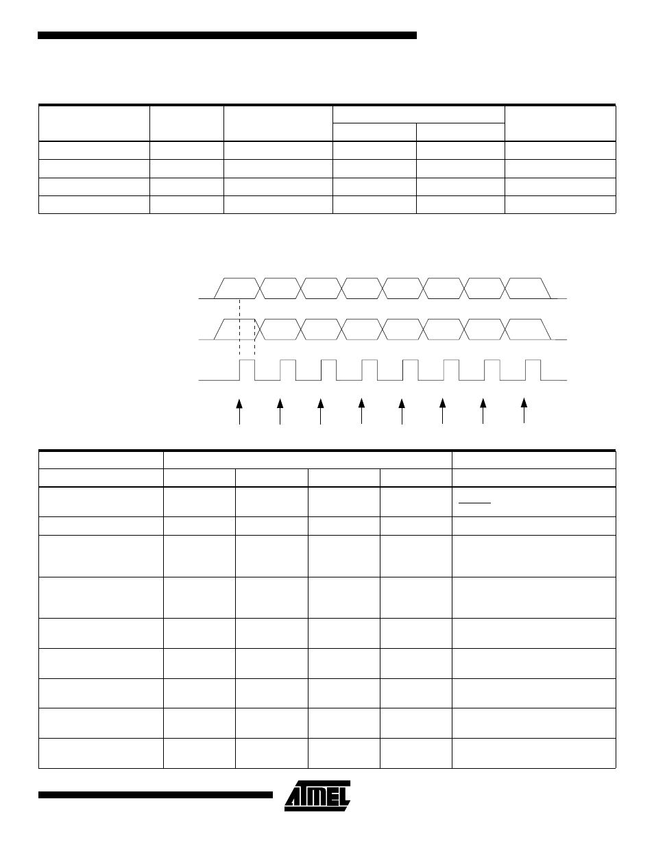
Figure 87. Serial Programming Waveforms
.
Table 59. Maximum Programming Times for Non-Volatile Memory
Operation
Symbol
Number of RC
oscillator cycles
Parallel / serial programming
Self programming
2.7V
5.0V
Chip Erase
t
WD_CE
16K
32 ms
30 ms
17 ms
Flash Write
t
WD_FLASH
8K
16 ms
15 ms
8.5 ms
EEPROM Write
t
WD_EEPROM
2K
4 ms
3.8 ms
2.2 ms
Fuse/lock bit write
t
WD_FUSE
1K
2 ms
1.9 ms
1.1 ms
MSB
MSB
LSB
LSB
SERIAL CLOCK INPUT
PB7(SCK)
SERIAL DATA INPUT
PB5 (MOSI)
PB6 (MISO)
SAMPLE
SERIAL DATA OUTPUT
Table 60. Serial Programming Instruction Set
Instruction
Instruction Format
Operation
Byte 1
Byte 2
Byte 3
Byte4
Programming Enable
1010 1100
0101 0011
xxxx xxxx
xxxx xxxx
Enable Serial Programming after
RESET goes low.
Chip Erase
1010 1100
100x xxxx
xxxx xxxx
xxxx xxxx
Chip Erase EEPROM and Flash.
Read Program Memory
0010 H000
xxxa aaaa
bbbb bbbb
oooo oooo
Read H (high or low) data o from
Program memory at word address
a:b.
Load Program Memory
Page
0100 H000
xxxx xxxx
xxbb bbbb
iiii iiii
Write H (high or low) data i to
Program Memory page at word
address b.
Write Program Memory
Page
0100 1100
xxxa aaaa
bb
xx xxxx
iiii iiii
Write Program Memory Page at
address a:b.
Read EEPROM Memory
1010 0000
xxxx xxxa
bbbb bbbb
oooo oooo
Read data o from EEPROM
memory at address a:b.
Write EEPROM Memory
1100 0000
xxxx xxxa
bbbb bbbb
iiii iiii
Write data i to EEPROM memory
at address a:b.
Read Lock Bits
0101 1000
xxxx xxxx
xxxx xxxx
xx65 4321
Read Lock bits. ‘0’ = programmed,
‘1’ = unprogrammed.
Write Lock Bits
1010 1100
111x xxxx
xxxx xxxx
1165 4321
Write Lock bits. Set bits 6 - 1 = ’0’ to
program Lock bits.