Timer/counter1 control register a - tccr1a, Atmega163(l) – Rainbow Electronics ATmega163L User Manual
Page 37
ATmega163(L)
37
The 16-bit Timer/Counter1 features both a high resolution and a high accuracy usage with the lower prescaling opportuni-
ties. Similarly, the high prescaling opportunities makes the Timer/Counter1 useful for lower speed functions or exact timing
functions with infrequent actions.
The Timer/Counter1 supports two Output Compare functions using the Output Compare Register 1 A and B (OCR1A and
OCR1B) as the data sources to be compared to the Timer/Counter1 contents. The Output Compare functions includes
optional clearing of the counter on compareA match, and actions on the Output Compare pins on both compare matches.
Timer/Counter1 can also be used as an 8, 9, or 10-bit Pulse Width Modulator. In this mode the counter and the
OCR1A/OCR1B registers serve as a dual glitch-free stand-alone PWM with centered pulses. Alternatively, the
Timer/Counter1 can be configured to operate at twice the speed in PWM mode, but without centered pulses. Refer to page
41 for a detailed description of this function.
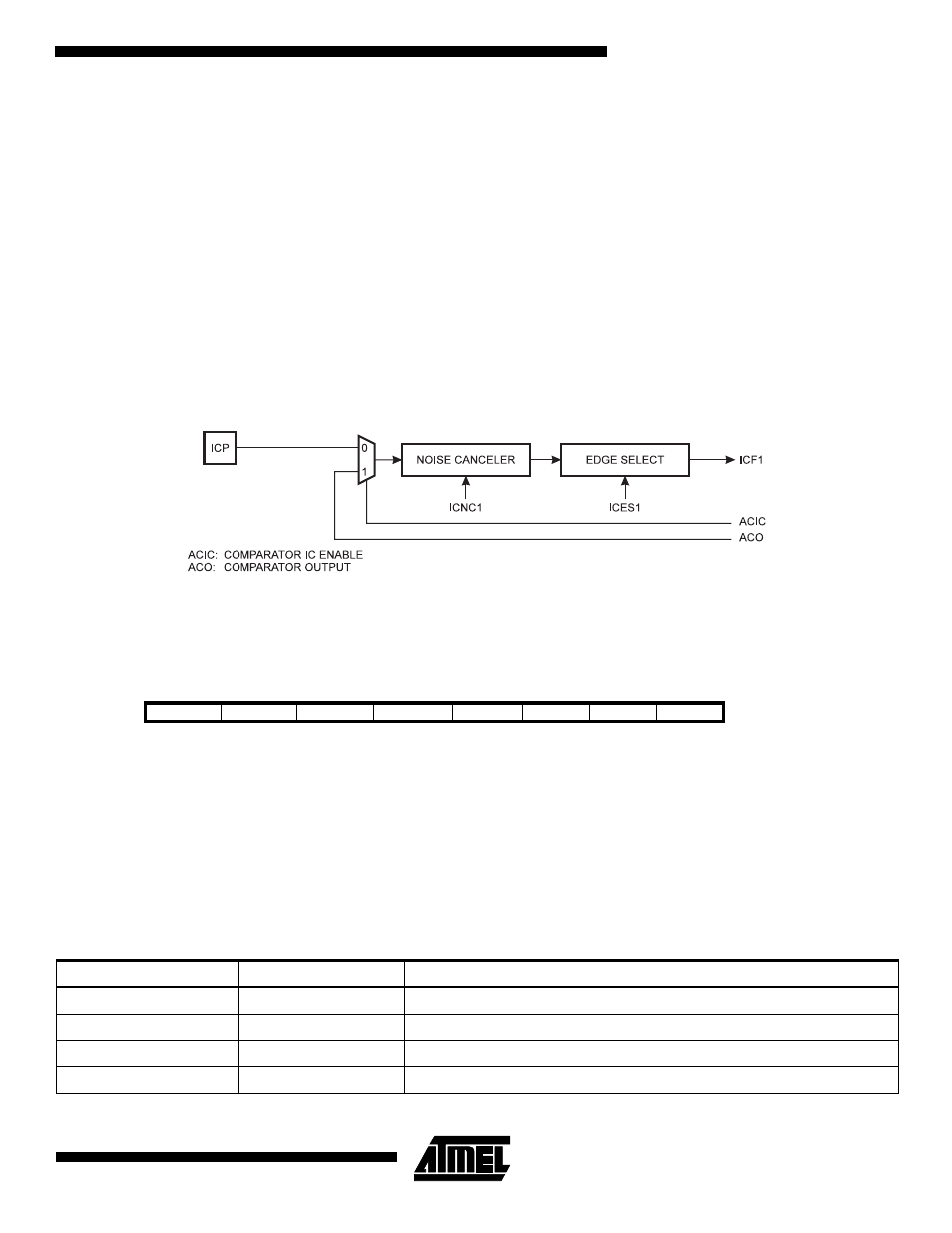
The Input Capture function of Timer/Counter1 provides a capture of the Timer/Counter1 contents to the Input Capture Reg-
ister - ICR1, triggered by an external event on the Input Capture Pin - ICP. The actual capture event settings are defined by
the Timer/Counter1 Control Register - TCCR1B. In addition, the Analog Comparator can be set to trigger the Input Capture.
Refer to the section, “The Analog Comparator”, for details on this. The ICP pin logic is shown in Figure 34.
Figure 34. ICP Pin Schematic Diagram
If the noise canceler function is enabled, the actual trigger condition for the capture event is monitored over 4 samples, and
all 4 must be equal to activate the capture flag.
Timer/Counter1 Control Register A - TCCR1A
•
Bits 7,6 - COM1A1, COM1A0: Compare Output Mode1A, Bits 1 and 0
The COM1A1 and COM1A0 control bits determine any output pin action following a compare match in Timer/Counter1.
Any output pin actions affect pin OC1A - Output CompareA. This is an alternative function to an I/O port, and the corre-
sponding direction control bit must be set (one) to control an output pin. The control configuration is shown in Table 10.
•
Bits 5,4 - COM1B1, COM1B0: Compare Output Mode1B, Bits 1 and 0
The COM1B1 and COM1B0 control bits determine any output pin action following a compare match in Timer/Counter1.
Any output pin actions affect pin OC1B - Output CompareB. This is an alternative function to an I/O port, and the corre-
sponding direction control bit must be set (one) to control an output pin. The control configuration is shown in Table 10.
Note:
X = A or B.
Bit
7
6
5
4
3
2
1
0
$2F ($4F)
COM1A1
COM1A0
COM1B1
COM1B0
FOC1A
FOC1B
PWM11
PWM10
TCCR1A
Read/Write
R/W
R/W
R/W
R/W
R/W
R/W
R/W
R/W
Initial value
0
0
0
0
0
0
0
0
Table 12. Compare 1 Mode Select
COM1X1
COM1X0
Description
0
0
Timer/Counter1 disconnected from output pin OC1X
0
1
Toggle the OC1X output line.
1
0
Clear the OC1X output line (to zero).
1
1
Set the OC1X output line (to one).