Port a schematics, Port b, Atmega163(l) – Rainbow Electronics ATmega163L User Manual
Page 100
ATmega163(L)
100
n: 7,6…0, pin number.
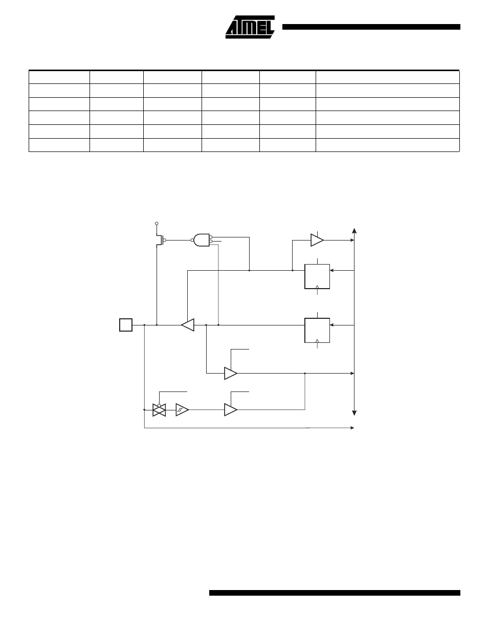
PORT A Schematics
Note that all port pins are synchronized. The synchronization latches are not shown in the figure.
Figure 63. PORTA Schematic Diagrams (Pins PA0 - PA7)
Port B
Port B is an 8-bit bi-directional I/O port with internal pull-ups.
Three I/O memory address locations are allocated for Port B, one each for the Data Register - PORTB, $18($38), Data
Direction Register - DDRB, $17($37) and the Port B Input Pins - PINB, $16($36). The Port B Input Pins address is read
only, while the Data Register and the Data Direction Register are read/write.
All port pins have individually selectable pull-up resistors. The Port B output buffers can sink 20mA and thus drive LED dis-
plays directly. When pins PB0 to PB7 are used as inputs and are externally pulled low, they will source current if the
internal pull-up resistors are activated.
Table 43. DDAn Effects on PORTA Pins
DDAn
PORTAn
PUD
I/O
Pull Up
Comment
0
0
x
Input
No
Tri-state (Hi-Z)
0
1
1
Input
No
Tri-state (Hi-Z)
0
1
0
Input
Yes
PAn will source current if ext. pulled low.
1
0
x
Output
No
Push-pull Zero Output
1
1
x
Output
No
Push-pull One Output
DA
T
A
BUS
D
D
Q
Q
RESET
RESET
C
C
WD
WP
RD
MOS
PULL-
UP
PDn
ADCn
TO ADC MUX
WP:
WD:
RL:
RP:
RD:
n:
WRITE PORTA
WRITE DDRA
READ PORTA LATCH
READ PORTA PIN
READ DDRA
0-7
DDAn
PORTAn
RL
RP
PWRDN
PUD
PUD: PULL-UP DISABLE