Operation, Atmega163(l), Can be selected as single ended inputs to the adc – Rainbow Electronics ATmega163L User Manual
Page 91
ATmega163(L)
91
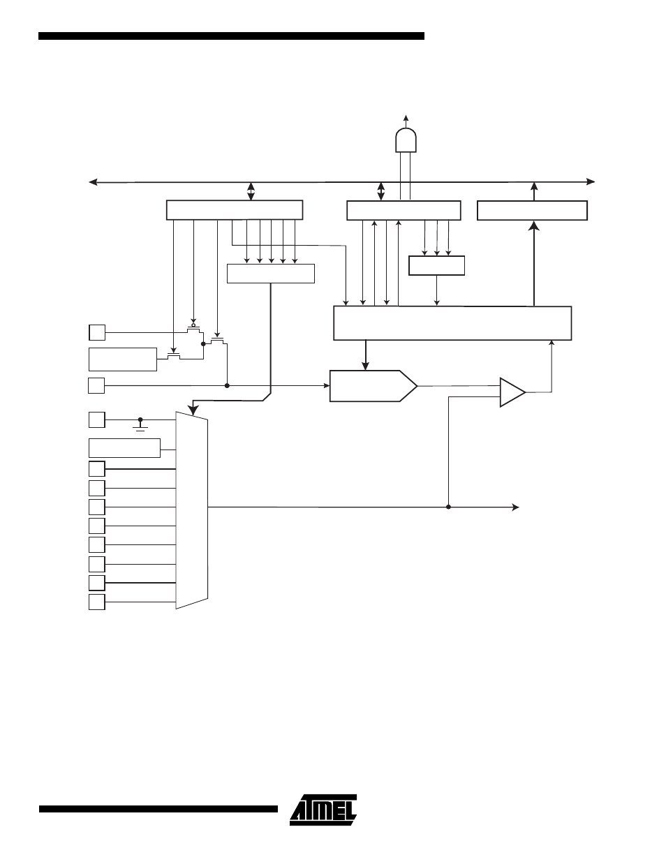
Figure 57. Analog to Digital Converter Block Schematic
Operation
The ADC converts an analog input voltage to a 10-bit digital value through successive approximation. The minimum value
represents AGND and the maximum value represents the voltage on the AREF pin minus 1 LSB. Optionally, AVCC or an
internal 2.56 V reference voltage may be connected to the AREF pin by writing to the REFSn bits in the ADMUX register.
The internal voltage reference may thus be decoupled by an external capacitor at the AREF pin to improve noise immunity.
The analog input channel is selected by writing to the MUX bits in ADMUX. Any of the eight ADC input pins ADC7..0, as
well as AGND and a fixed bandgap voltage reference of nominally 1.22 V (V
BG
), can be selected as single ended inputs to
the ADC.
ADC CONVERSION
COMPLETE IRQ
8-BIT DATA BUS
15
0
ADC MULTIPLEXER
SELECT (ADMUX)
ADC CTRL. & STATUS
REGISTER (ADCSR)
ADC DATA REGISTER
(ADCH/ADCL)
MUX2
ADIE
ADFR
ADSC
ADEN
ADIF
ADIF
MUX1
MUX0
ADPS0
ADPS1
ADPS2
CONVERSION LOGIC
10-BIT DAC
+
-
SAMPLE & HOLD
COMPARATOR
INTERNAL 2.56 V
REFERENCE
MUX DECODER
AVCC
REFS0
REFS1
ADLAR
CHANNEL SELECTION
ADC[9:0]
ADC MULTIPLEXER
OUTPUT
AREF
PRESCALER
ADC7
ADC6
ADC5
ADC4
ADC3
ADC2
ADC1
ADC0
1.22 V BANDGAP
REFERENCE
AGND
INPUT
MUX
MUX3
MUX4