Alternate functions of portd, Port d schematics, Atmega163(l) – Rainbow Electronics ATmega163L User Manual
Page 111
ATmega163(L)
111
pin has to be configured as an output pin, or the PUD bit has to be set. The Port D pins are tri-stated when a reset condition
becomes active, even if the clock is not running.
n: 7,6…0, pin number.
Alternate Functions Of PORTD
•
OC2 - PORTD, Bit 7
OC2, Timer/Counter2 output compare match output: The PD7 pin can serve as an external output for the Timer/Counter2
output compare. The pin has to be configured as an output (DDD7 set (one)) to serve this function. See the timer descrip-
tion on how to enable this function. The OC2 pin is also the output pin for the PWM mode timer function.
•
ICP - PORTD, Bit 6
ICP - Input Capture Pin: The PD6 pin can act as an input capture pin for Timer/Counter1. The pin has to be configured as
an input (DDD6 cleared(zero)) to serve this function. See the timer description on how to enable this function.
•
OC1A - PORTD, Bit 5
OC1A, Output compare matchA output: The PD5 pin can serve as an external output for the Timer/Counter1 output com-
pareA. The pin has to be configured as an output (DDD5 set (one)) to serve this function. See the timer description on how
to enable this function. The OC1A pin is also the output pin for the PWM mode timer function.
•
OC1B - PORTD, Bit 4
OC1B, Output compare matchB output: The PD4 pin can serve as an external output for the Timer/Counter1 output com-
pareB. The pin has to be configured as an output (DDD4 set (one)) to serve this function. See the timer description on how
to enable this function. The OC1B pin is also the output pin for the PWM mode timer function.
•
INT1 - PORTD, Bit 3
INT1, External Interrupt source 1: The PD3 pin can serve as an external interrupt source to the MCU. See the interrupt
description for further details, and how to enable the source.
•
INT0 - PORTD, Bit 2
INT0, External Interrupt source 0: The PD2 pin can serve as an external interrupt source to the MCU. See the interrupt
description for further details, and how to enable the source.
•
TXD - Port D, Bit 1
TXD, Transmit Data (Data output pin for the UART). When the UART transmitter is enabled, this pin is configured as an
output regardless of the value of DDRD1.
•
RXD - Port D, Bit 0
RXD, Receive Data (Data input pin for the UART). When the UART receiver is enabled this pin is configured as an input
regardless of the value of DDRD0. When the UART forces this pin to be an input, a logical one in PORTD0 will turn on the
internal pull-up.
Port D Schematics
Note that all port pins are synchronized. The synchronization latches are not shown in the figures.
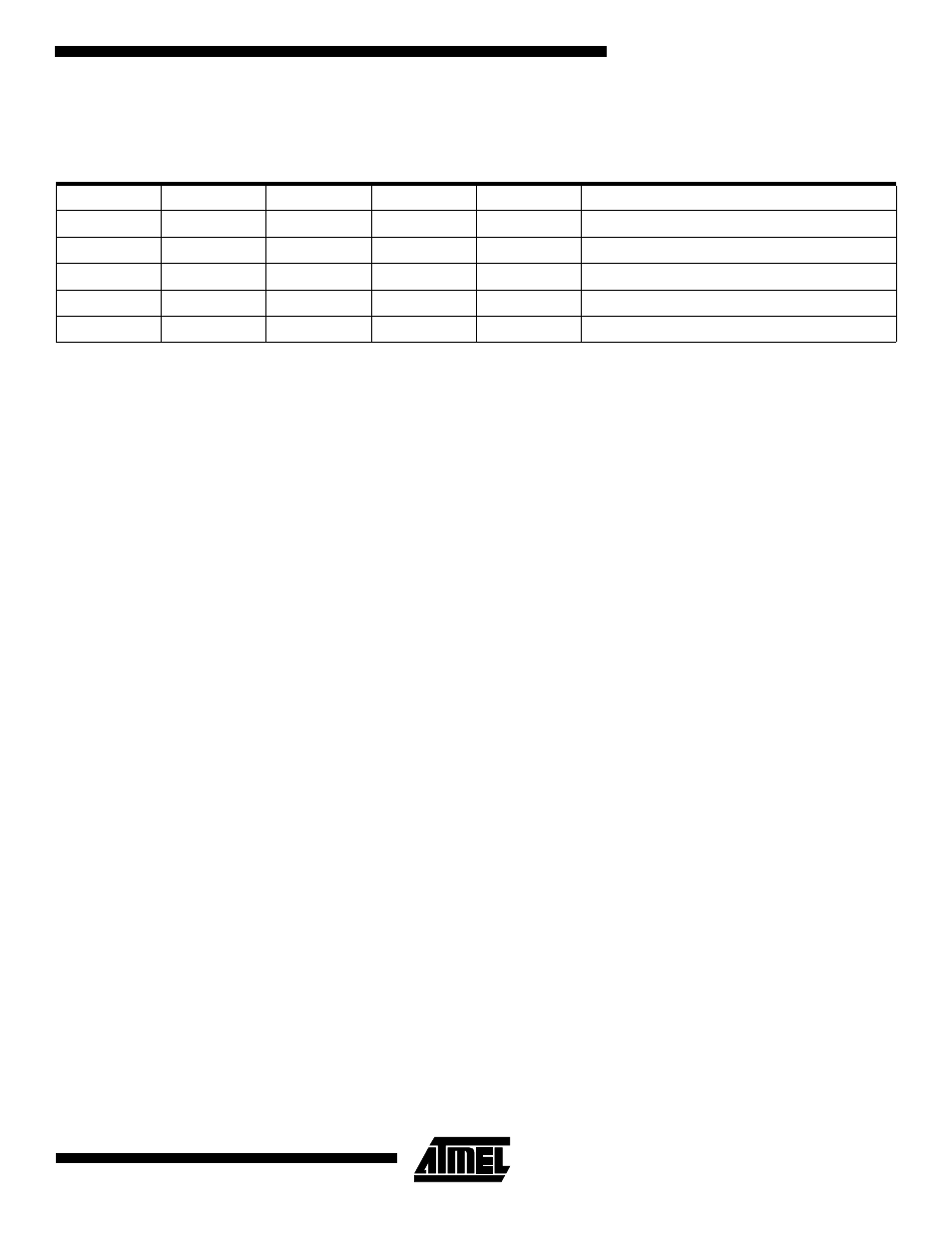
Table 49. DDDn Bits on Port D Pins
DDDn
PORTDn
PUD
I/O
Pull Up
Comment
0
0
x
Input
No
Tri-state (Hi-Z)
0
1
1
Input
No
Tri-state (Hi-Z)
0
1
0
Input
Yes
PDn will source current if ext. pulled low.
1
0
x
Output
No
Push-pull Zero Output
1
1
x
Output
No
Push-pull One Output