Timer/counter1 control register b - tccr1b, Atmega163(l) – Rainbow Electronics ATmega163L User Manual
Page 38
ATmega163(L)
38
In PWM mode, these bits have a different function. Refer to Table 14 for a detailed description.
•
Bit 3 - FOC1A: Force Output Compare1A
Writing a logical one to this bit, forces a change in the compare match output pin PD5 according to the values already set in
COM1A1 and COM1A0. If the COM1A1 and COM1A0 bits are written in the same cycle as FOC1A, the new settings will
not take effect until next compare match or forced compare match occurs. The Force Output Compare bit can be used to
change the output pin without waiting for a compare match in the timer. The automatic action programmed in COM1A1 and
COM1A0 happens as if a Compare Match had occurred, but no interrupt is generated and it will not clear the timer even if
CTC1 in TCCR1B is set. The corresponding I/O pin must be set as an output pin for the FOC1A bit to have effect on the
pin. The FOC1A bit will always be read as zero. The setting of the FOC1A bit has no effect in PWM mode.
•
Bit 2 - FOC1B: Force Output Compare1B
Writing a logical one to this bit, forces a change in the compare match output pin PD4 according to the values already set in
COM1B1 and COM1B0. If the COM1B1 and COM1B0 bits are written in the same cycle as FOC1B, the new settings will
not take effect until next compare match or forced compare match occurs. The Force Output Compare bit can be used to
change the output pin without waiting for a compare match in the timer. The automatic action programmed in COM1B1 and
COM1B0 happens as if a Compare Match had occurred, but no interrupt is generated. The corresponding I/O pin must be
set as an output pin for the FOC1B bit to have effect on the pin. The FOC1B bit will always be read as zero. The setting of
the FOC1B bit has no effect in PWM mode.
•
Bits 1..0 - PWM11, PWM10: Pulse Width Modulator Select Bits
These bits select PWM operation of Timer/Counter1 as specified in Table 11. This mode is described on page 41.
Timer/Counter1 Control Register B - TCCR1B
•
Bit 7 - ICNC1: Input Capture1 Noise Canceler (4 CKs)
When the ICNC1 bit is cleared (zero), the input capture trigger noise canceler function is disabled. The input capture is trig-
gered at the first rising/falling edge sampled on the ICP - input capture pin - as specified. When the ICNC1 bit is set (one),
four successive samples are measures on the ICP - input capture pin, and all samples must be high/low according to the
input capture trigger specification in the ICES1 bit. The actual sampling frequency is XTAL clock frequency.
•
Bit 6 - ICES1: Input Capture1 Edge Select
While the ICES1 bit is cleared (zero), the Timer/Counter1 contents are transferred to the Input Capture Register - ICR1 - on
the falling edge of the input capture pin - ICP. While the ICES1 bit is set (one), the Timer/Counter1 contents are transferred
to the Input Capture Register - ICR1 - on the rising edge of the input capture pin - ICP.
•
Bits 5, 4 - Res: Reserved Bits
These bits are reserved bits in the ATmega163 and always read as zero.
•
Bit 3 - CTC1: Clear Timer/Counter1 on Compare Match
When the CTC1 control bit is set (one), the Timer/Counter1 is reset to $0000 in the clock cycle after a compareA match. If
the CTC1 control bit is cleared, Timer/Counter1 continues counting and is unaffected by a compare match. When a pres-
caling of 1 is used, and the compareA register is set to C, the timer will count as follows if CTC1 is set:
... | C-1 | C | 0 | 1 |...
When the prescaler is set to divide by 8, the timer will count like this:
Table 13. PWM Mode Select
PWM11
PWM10
Description
0
0
PWM operation of Timer/Counter1 is disabled
0
1
Timer/Counter1 is an 8-bit PWM
1
0
Timer/Counter1 is a 9-bit PWM
1
1
Timer/Counter1 is a 10-bit PWM
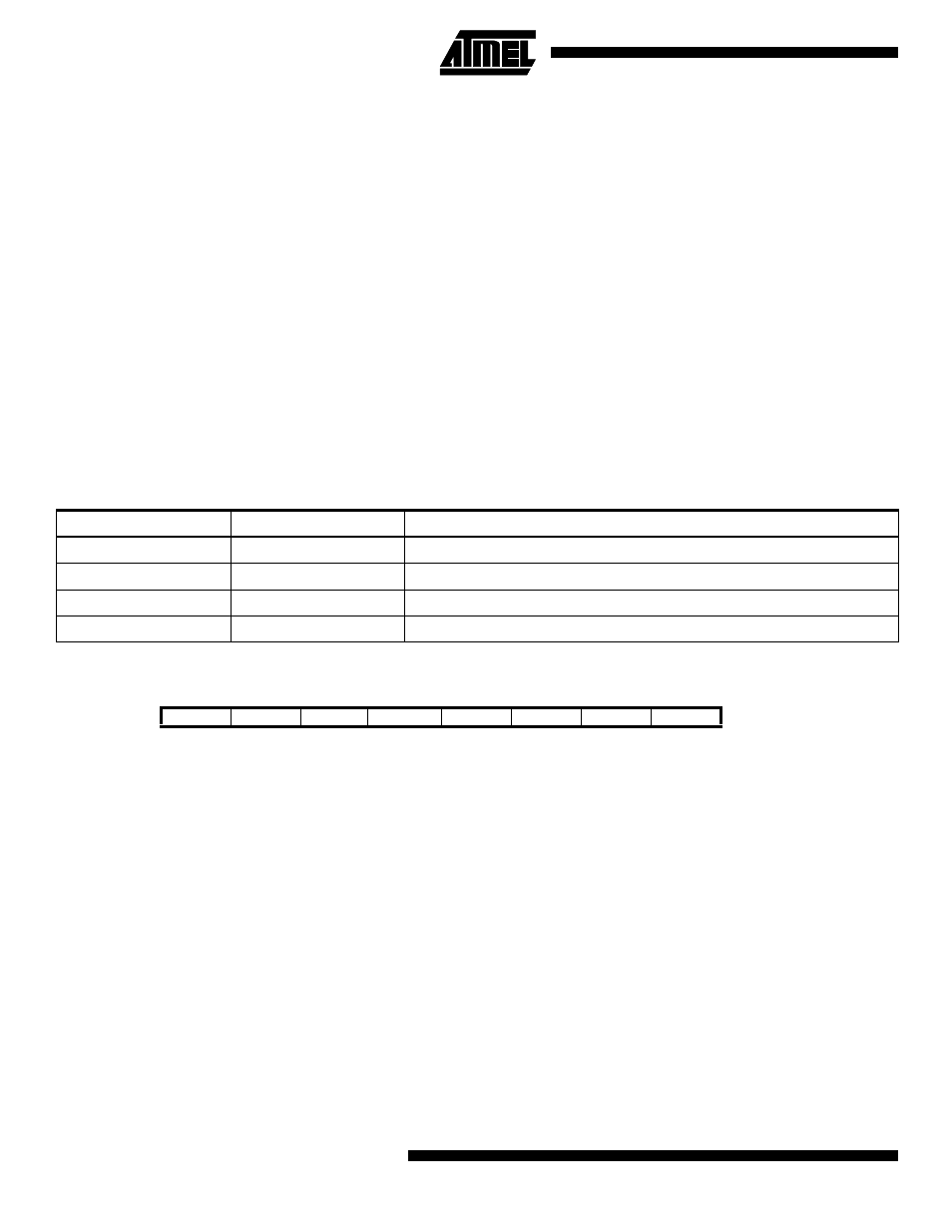
Bit
7
6
5
4
3
2
1
0
$2E ($4E)
ICNC1
ICES1
-
-
CTC1
CS12
CS11
CS10
TCCR1B
Read/Write
R/W
R/W
R
R
R/W
R/W
R/W
R/W
Initial value
0
0
0
0
0
0
0
0