The port b data register - portb, The port b data direction register - ddrb, The port b input pins address - pinb – Rainbow Electronics ATmega163L User Manual
Page 101: Port b as general digital i/o, Atmega163(l)
ATmega163(L)
101
The Port B pins with alternate functions are shown in Table 44.
When the pins are used for the alternate function, the DDRB and PORTB registers have to be set according to the alternate
function description.
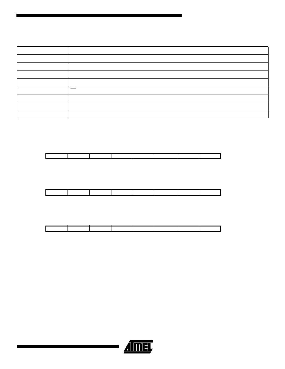
The Port B Data Register - PORTB
The Port B Data Direction Register - DDRB
The Port B Input Pins Address - PINB
The Port B Input Pins address - PINB - is not a register, and this address enables access to the physical value on each Port
B pin. When reading PORTB, the PORTB Data Latch is read, and when reading PINB, the logical values present on the
pins are read.
Port B As General Digital I/O
All 8 bits in Port B are equal when used as digital I/O pins. PBn, General I/O pin: The DDBn bit in the DDRB register selects
the direction of this pin, if DDBn is set (one), PBn is configured as an output pin. If DDBn is cleared (zero), PBn is config-
ured as an input pin. If PORTBn is set (one) when the pin configured as an input pin, the MOS pull up resistor is activated.
To switch the pull up resistor off, the PORTBn has to be cleared (zero), the pin has to be configured as an output pin, or the
PUD bit has to be set. The Port B pins are tri-stated when a reset condition becomes active, even if the clock is not running.
Table 44. Port B Pins Alternate Functions
Port Pin
Alternate Functions
PB0
T0 (Timer/Counter 0 External Counter Input)
PB1
T1 (Timer/Counter 1 External Counter Input)
PB2
AIN0 (Analog Comparator Positive Input)
PB3
AIN1 (Analog Comparator Negative Input)
PB4
SS (SPI Slave Select Input)
PB5
MOSI (SPI Bus Master Output/Slave Input)
PB6
MISO (SPI Bus Master Input/Slave Output)
PB7
SCK (SPI Bus Serial Clock)
Bit
7
6
5
4
3
2
1
0
$18 ($38)
PORTB7
PORTB6
PORTB5
PORTB4
PORTB3
PORTB2
PORTB1
PORTB0
PORTB
Read/Write
R/W
R/W
R/W
R/W
R/W
R/W
R/W
R/W
Initial value
0
0
0
0
0
0
0
0
Bit
7
6
5
4
3
2
1
0
$17 ($37)
DDB7
DDB6
DDB5
DDB4
DDB3
DDB2
DDB1
DDB0
DDRB
Read/Write
R/W
R/W
R/W
R/W
R/W
R/W
R/W
R/W
Initial value
0
0
0
0
0
0
0
0
Bit
7
6
5
4
3
2
1
0
$16 ($36)
PINB7
PINB6
PINB5
PINB4
PINB3
PINB2
PINB1
PINB0
PINB
Read/Write
R
R
R
R
R
R
R
R
Initial value
N/A
N/A
N/A
N/A
N/A
N/A
N/A
N/A