The status register - sreg, Atmega163(l) – Rainbow Electronics ATmega163L User Manual
Page 18
ATmega163(L)
18
Note:
Reserved and unused locations are not shown in the table.
All ATmega163 I/Os and peripherals are placed in the I/O space. The I/O locations are accessed by the IN and OUT
instructions, transferring data between the 32 general purpose working registers and the I/O space. I/O registers within the
address range $00 - $1F are directly bit-accessible using the SBI and CBI instructions. In these registers, the value of sin-
gle bits can be checked by using the SBIS and SBIC instructions. Refer to the instruction set chapter for more details.
When using the I/O specific commands IN and OUT, the I/O addresses $00 - $3F must be used. When addressing I/O reg-
isters as SRAM, $20 must be added to these addresses. All I/O register addresses throughout this document are shown
with the SRAM address in parentheses.
For compatibility with future devices, reserved bits should be written to zero if accessed. Reserved I/O memory addresses
should never be written.
Some of the status flags are cleared by writing a logical one to them. Note that the CBI and SBI instructions will operate on
all bits in the I/O register, writing a one back into any flag read as set, thus clearing the flag. The CBI and SBI instructions
work with registers $00 to $1F only.
The I/O and peripherals control registers are explained in the following sections.
The Status Register - SREG
The AVR status register - SREG - at I/O space location $3F ($5F) is defined as:
•
Bit 7 - I: Global Interrupt Enable
The global interrupt enable bit must be set (one) for the interrupts to be enabled. The individual interrupt enable control is
then performed in the interrupt mask registers. If the global interrupt enable register is cleared (zero), none of the interrupts
are enabled independent of the values of the interrupt mask registers. The I-bit is cleared by hardware after an interrupt has
occurred, and is set by the RETI instruction to enable subsequent interrupts.
•
Bit 6 - T: Bit Copy Storage
The bit copy instructions BLD (Bit LoaD) and BST (Bit STore) use the T bit as source and destination for the operated bit. A
bit from a register in the register file can be copied into T by the BST instruction, and a bit in T can be copied into a bit in a
register in the register file by the BLD instruction.
•
Bit 5 - H: Half Carry Flag
The half carry flag H indicates a half carry in some arithmetic operations. See the Instruction Set Description for detailed
information.
•
Bit 4 - S: Sign Bit, S = N
=⊕
V
The S-bit is always an exclusive or between the negative flag N and the two’s complement overflow flag V. See the Instruc-
tion Set Description for detailed information.
•
Bit 3 - V: Two’s Complement Overflow Flag
The two’s complement overflow flag V supports two’s complement arithmetics. See the Instruction Set Description for
detailed information.
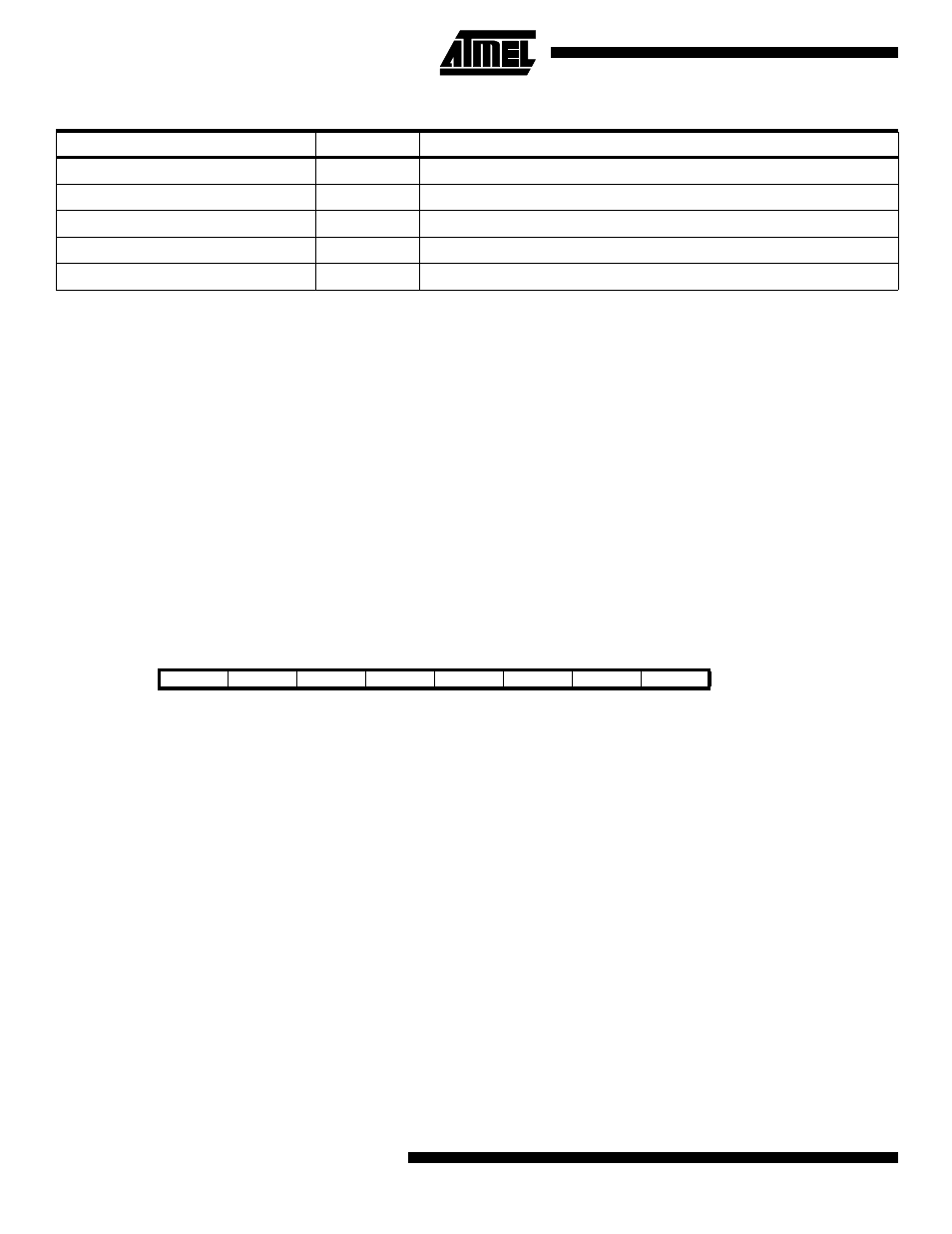
$04 ($24)
ADCL
ADC Data Register Low
$03 ($23)
TWDR
2-wire Serial Interface Data Register
$02 ($22)
TWAR
2-wire Serial Interface (Slave) Address Register
$01 ($21)
TWSR
2-wire Serial Interface Status Register
$00 ($20)
TWBR
2-wire Serial Interface Bit Rate Register
Bit
7
6
5
4
3
2
1
0
$3F ($5F)
I
T
H
S
V
N
Z
C
SREG
Read/Write
R/W
R/W
R/W
R/W
R/W
R/W
R/W
R/W
Initial value
0
0
0
0
0
0
0
0
Table 2. ATmega163 I/O Space (Continued)
I/O Address (SRAM Address)
Name
Function