Port c, The port c data register - portc, The port c data direction register - ddrc – Rainbow Electronics ATmega163L User Manual
Page 106: The port c input pins address - pinc, Port c as general digital i/o, Atmega163(l)
ATmega163(L)
106
Port C
Port C is an 8-bit bi-directional I/O port with internal pull-ups.
Three I/O memory address locations are allocated for the Port C, one each for the Data Register - PORTC, $15($35), Data
Direction Register - DDRC, $14($34) and the Port C Input Pins - PINC, $13($33). The Port C Input Pins address is read
only, while the Data Register and the Data Direction Register are read/write.
All port pins have individually selectable pull-up resistors. The PORT C output buffers can sink 20 mA and thus drive LED
displays directly. When pins PC0 to PC7 are used as inputs and are externally pulled low, they will source current if the
internal pull-up resistors are activated.
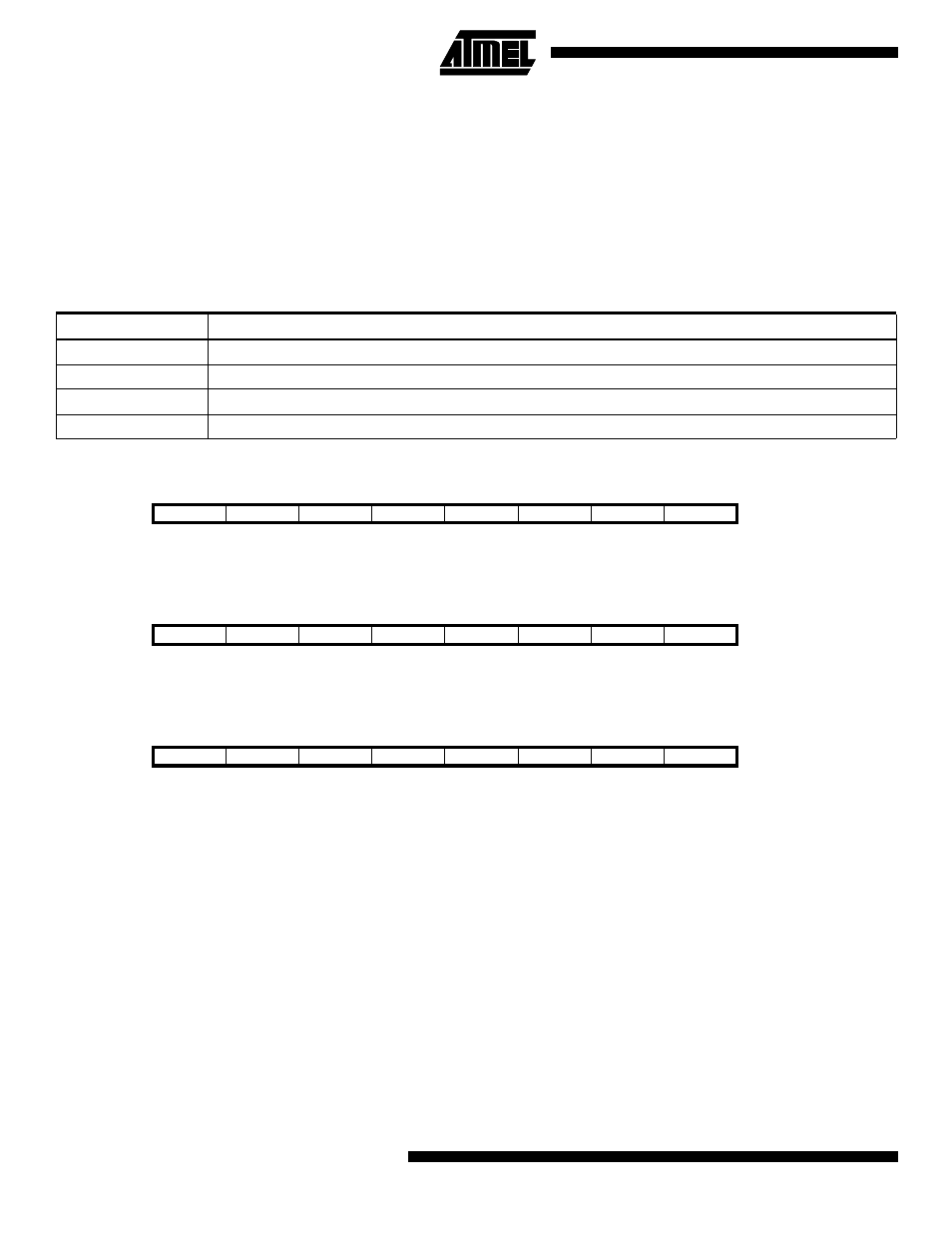
The Port C Data Register - PORTC
The Port C Data Direction Register - DDRC
The Port C Input Pins Address - PINC
The Port C Input Pins address - PINC - is not a register, and this address enables access to the physical value on each
Port C pin. When reading PORTC, the PORTC Data Latch is read, and when reading PINC, the logical values present on
the pins are read.
Port C As General Digital I/O
All 8 bits in PORT C are equal when used as digital I/O pins.
PCn, General I/O pin: The DDCn bit in the DDRC register selects the direction of this pin, if DDCn is set (one), PCn is con-
figured as an output pin. If DDCn is cleared (zero), PCn is configured as an input pin. If PORTCn is set (one) when the pin
configured as an input pin, the MOS pull up resistor is activated. To switch the pull up resistor off, PORTCn has to be
cleared (zero), the pin has to be configured as an output pin, or the PUD bit has to be set. The Port C pins are tri-stated
when a reset condition becomes active, even if the clock is not running.
Table 46. Port C Pins Alternate Functions
Port Pin
Alternate Function
PC0
SCL (2-wire Serial Bus Clock Line)
PC1
SDA (2-wire Serial Bus Data Input/Output Line)
PC6
TOSC1 (Timer Oscillator Pin 1)
PC7
TOSC2 (Timer Oscillator Pin 2)
Bit
7
6
5
4
3
2
1
0
$15 ($35)
PORTC7
PORTC6
PORTC5
PORTC4
PORTC3
PORTC2
PORTC1
PORTC0
PORTC
Read/Write
R/W
R/W
R/W
R/W
R/W
R/W
R/W
R/W
Initial value
0
0
0
0
0
0
0
0
Bit
7
6
5
4
3
2
1
0
$14 ($34)
DDC7
DDC6
DDC5
DDC4
DDC3
DDC2
DDC1
DDC0
DDRC
Read/Write
R/W
R/W
R/W
R/W
R/W
R/W
R/W
R/W
Initial value
0
0
0
0
0
0
0
0
Bit
7
6
5
4
3
2
1
0
$13 ($33)
PINC7
PINC6
PINC5
PINC4
PINC3
PINC2
PINC1
PINC0
PINC
Read/Write
R
R
R
R
R
R
R
R
Initial value
N/A
N/A
N/A
N/A
N/A
N/A
N/A
N/A