Timer/counter0 control register - tccr0, Figure 32, Atmega163(l) – Rainbow Electronics ATmega163L User Manual
Page 35: Table 11. clock 0 prescale select
ATmega163(L)
35
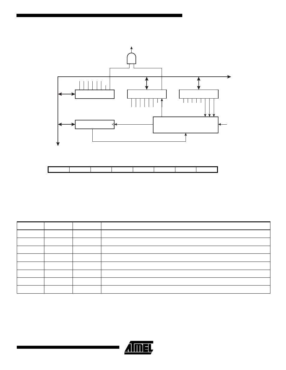
Figure 32. Timer/Counter0 Block Diagram
Timer/Counter0 Control Register - TCCR0
•
Bits 7..3 - Res: Reserved Bits
These bits are reserved bits in the ATmega163 and always read as zero.
•
Bits 2..0 - CS02, CS01, CS00: Clock Select0, Bit 2,1, and 0
The Clock Select0 bits 2,1, and 0 define the prescaling source of Timer0.
The Stop condition provides a Timer Enable/Disable function. The prescaled CK modes are scaled directly from the CK
oscillator clock. If the external pin modes are used for Timer/Counter0, transitions on PB0/(T0) will clock the counter even if
the pin is configured as an output. This feature can give the user SW control of the counting.
Bit
7
6
5
4
3
2
1
0
$33 ($53)
-
-
-
-
-
CS02
CS01
CS00
TCCR0
Read/Write
R
R
R
R
R
R/W
R/W
R/W
Initial value
0
0
0
0
0
0
0
0
Table 11. Clock 0 Prescale Select
CS02
CS01
CS00
Description
0
0
0
Stop, Timer/Counter0 is stopped.
0
0
1
CK
0
1
0
CK / 8
0
1
1
CK / 64
1
0
0
CK / 256
1
0
1
CK / 1024
1
1
0
External Pin T0, falling edge
1
1
1
External Pin T0, rising edge
8-BIT DA
T
A
BUS
T/C0 CONTROL
REGISTER (TCCR0)
TIMER/COUNTER0
(TCNT0)
0
7
T/C CLK SOURCE
CONTROL
LOGIC
CS02
CS01
CS00
CK
T/C0 OVER-
FLOW IRQ
TIMER INT. MASK
REGISTER (TIMSK)
TOIE0
TOIE1
OCIE1A
OCIE1B
TICIE1
TOIE2
OCIE2
TIMER INT. FLAG
REGISTER (TIFR)
TOV0
TOV1
OCF1A
OCF1B
ICF1
TOV2
OCF2