Timer/counter2 - tcnt2, Timer/counter2 output compare register - ocr2, Timer/counter2 in pwm mode – Rainbow Electronics ATmega163L User Manual
Page 46: Pwm modes (up/down and overflow), Atmega163(l)
ATmega163(L)
46
The Stop condition provides a Timer Enable/Disable function. The prescaled modes are scaled directly from the PCK2
clock.
Timer/Counter2 - TCNT2
This 8-bit register contains the value of Timer/Counter2.
Timer/Counters2 is implemented as an up or up/down (in PWM mode) counter with read and write access. If the
Timer/Counter2 is written to and a clock source is selected, it continues counting in the timer clock cycle following the write
operation.
Timer/Counter2 Output Compare Register - OCR2
The output compare register is an 8-bit read/write register.
The Timer/Counter Output Compare Register contains the data to be continuously compared with Timer/Counter2. Actions
on compare matches are specified in TCCR2. A compare match does only occur if Timer/Counter2 counts to the OCR2
value. A software write that sets TCNT2 and OCR2 to the same value does not generate a compare match.
A compare match will set the compare interrupt flag in the CPU clock cycle following the compare event.
Timer/Counter2 in PWM Mode
When PWM mode is selected, the Timer/Counter2 either wraps (overflows) when it reaches $FF or it acts as an up/down
counter.
If the up/down mode is selected, the Timer/Counter2 and the Output Compare Register - OCR2 form an 8-bit, free-running,
glitch-free, and phase correct PWM with outputs on the PD7(OC2) pin.
If the overflow mode is selected, the Timer/Counter2 and the Output Compare Register - OCR2 form an 8-bit, free-running,
and glitch-free PWM, operating with twice the speed of the up/down counting mode.
PWM Modes (Up/Down and Overflow)
The two different PWM modes are selected by the CTC2 bit in the Timer/Counter Control Register - TCCR2.
If CTC2 is cleared and PWM mode is selected, the Timer/Counter acts as an up/down counter, counting up from $00 to
$FF, where it turns and counts down again to zero before the cycle is repeated. When the counter value matches the con-
tents of the Output Compare Register, the PD7(OC2) pin is set or cleared according to the settings of the COM21/COM20
bits in the Timer/Counter Control Register TCCR2.
1
0
0
PCK2 / 64
1
0
1
PCK2 / 128
1
1
0
PCK2 / 256
1
1
1
PCK2 / 1024
Bit
7
6
5
4
3
2
1
0
$24 ($44)
MSB
LSB
TCNT2
Read/Write
R/W
R/W
R/W
R/W
R/W
R/W
R/W
R/W
Initial value
0
0
0
0
0
0
0
0
Bit
7
6
5
4
3
2
1
0
$23 ($43)
MSB
LSB
OCR2
Read/Write
R/W
R/W
R/W
R/W
R/W
R/W
R/W
R/W
Initial value
0
0
0
0
0
0
0
0
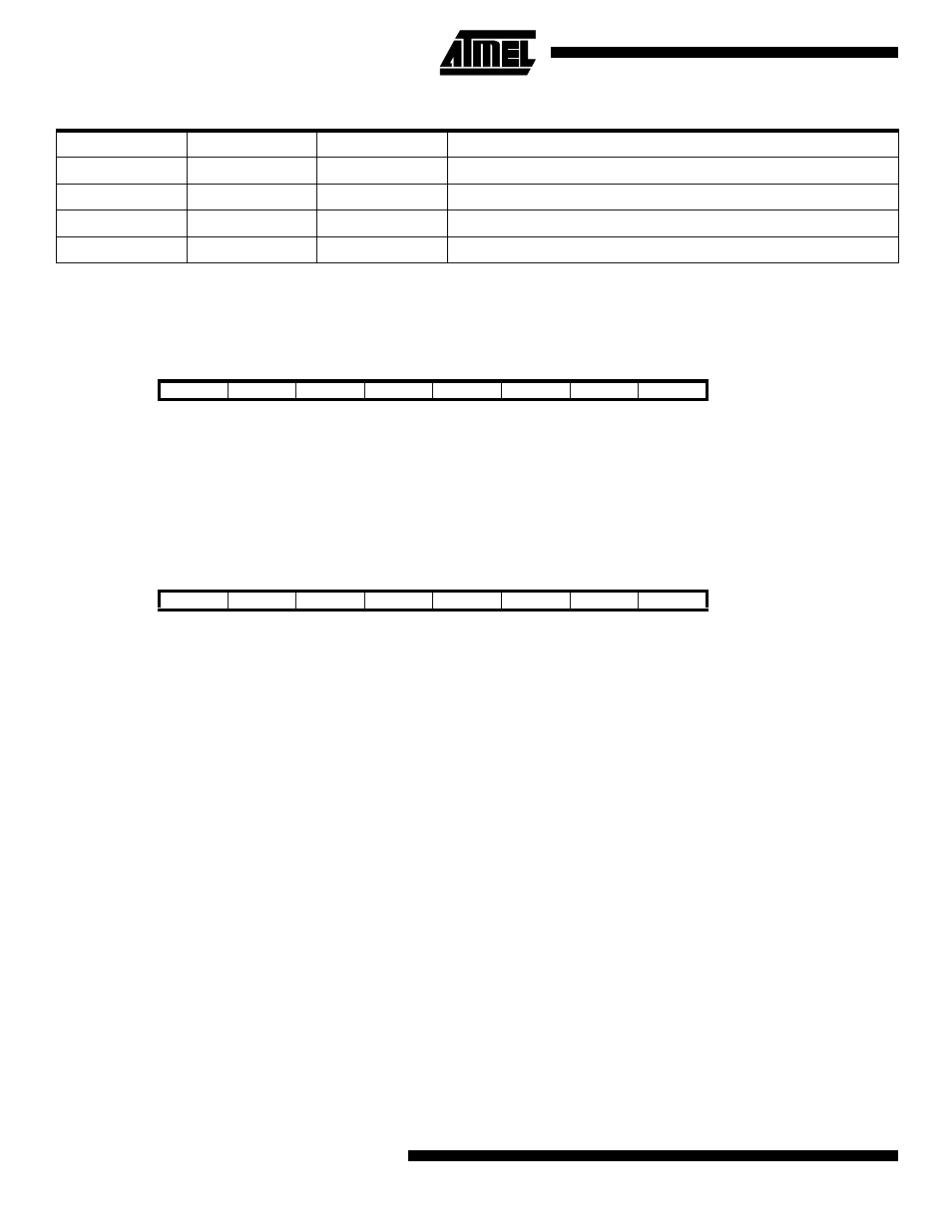
Table 20. Timer/Counter2 Prescale Select (Continued)
CS22
CS21
CS20
Description