The adc multiplexer selection register - admux, Atmega163(l) – Rainbow Electronics ATmega163L User Manual
Page 95
ATmega163(L)
95
The ADC Multiplexer Selection Register - ADMUX
•
Bit 7,6 - REFS1..0: Reference Selection Bits
These bits select the voltage reference for the ADC, as shown in Table 17. If these bits are changed during a conversion,
the change will not go in effect until this conversion is complete (ADIF in ADCSR is set). The user should disregard the first
conversion result after changing these bits to obtain maximum accuracy. The internal voltage reference options may not be
used if an external reference voltage is being applied to the AREF pin.
•
Bit 5 - ADLAR: ADC Left Adjust Result
The ADLAR bit affects the presentation of the ADC conversion result in the ADC data register. If ADLAR is cleared, the
result is right adjusted. If ADLAR is set, the result is left adjusted. Changing the ADLAR bit will affect the ADC data register
immediately, regardless of any ongoing conversions. For a complete description of this bit, see “The ADC Data Register -
ADCL and ADCH” on page 97.
•
Bits 4..0 - MUX4..MUX0: Analog Channel and Gain Selection Bits
The value of these bits selects which combination of analog inputs are connected to the ADC. See Table 41 for details. If
these bits are changed during a conversion, the change will not go in effect until this conversion is complete (ADIF in
ADCSR is set).
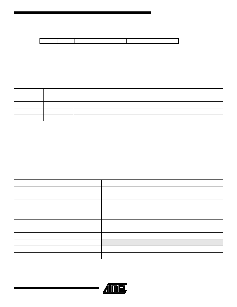
Bit
7
6
5
4
3
2
1
0
$07 ($27)
REFS1
REFS0
ADLAR
MUX4
MUX3
MUX2
MUX1
MUX0
ADMUX
Read/Write
R/W
R/W
R/W
R/W
R/W
R/W
R/W
R/W
Initial value
0
0
0
0
0
0
0
0
Table 40. Voltage Reference Selections for ADC
REFS1
REFS0
Voltage Reference Selection
0
0
AREF, Internal Vref turned off
0
1
AVCC with external capacitor at AREF pin
1
0
Reserved
1
1
Internal 2.56V Voltage Reference with external capacitor at AREF pin
Table 41. Input Channel Selections
MUX4..0
Single-ended Input
00000
ADC0
00001
ADC1
00010
ADC2
00011
ADC3
00100
ADC4
00101
ADC5
00110
ADC6
00111
ADC7
01000..11101
Reserved
11110
1.22V (V
BG
)
11111
0V (AGND)