Alternate functions of portb, Port b schematics, Atmega163(l) – Rainbow Electronics ATmega163L User Manual
Page 102
ATmega163(L)
102
n: 7,6…0, pin number.
Alternate Functions Of PORTB
The alternate pin configuration is as follows:
•
SCK - PORTB, Bit 7
SCK: Master clock output, slave clock input pin for SPI channel. When the SPI is enabled as a slave, this pin is configured
as an input regardless of the setting of DDB7. When the SPI is enabled as a master, the data direction of this pin is con-
trolled by DDB7. When the pin is forced to be an input, the pull-up can still be controlled by the PORTB7 bit. See the
description of the SPI port for further details.
•
MISO - PORTB, Bit 6
MISO: Master data input, slave data output pin for SPI channel. When the SPI is enabled as a master, this pin is configured
as an input regardless of the setting of DDB6. When the SPI is enabled as a slave, the data direction of this pin is controlled
by DDB6. When the pin is forced to be an input, the pull-up can still be controlled by the PORTB6 bit. See the description of
the SPI port for further details.
•
MOSI - PORTB, Bit 5
MOSI: SPI Master data output, slave data input for SPI channel. When the SPI is enabled as a slave, this pin is configured
as an input regardless of the setting of DDB5. When the SPI is enabled as a master, the data direction of this pin is con-
trolled by DDB5. When the pin is forced to be an input, the pull-up can still be controlled by the PORTB5 bit. See the
description of the SPI port for further details.
•
SS - PORTB, Bit 4
SS: Slave port select input. When the SPI is enabled as a slave, this pin is configured as an input regardless of the setting
of DDB4. As a slave, the SPI is activated when this pin is driven low. When the SPI is enabled as a master, the data direc-
tion of this pin is controlled by DDB4. When the pin is forced to be an input, the pull-up can still be controlled by the
PORTB4 bit. See the description of the SPI port for further details.
•
AIN1 - PORTB, Bit 3
AIN1, Analog Comparator Negative Input. When configured as an input (DDB3 is cleared (zero)) and with the internal MOS
pull up resistor switched off (PB3 is cleared (zero)), this pin also serves as the negative input of the on-chip analog compar-
ator. During power down mode, the schmitt trigger of the digital input is disconnected. This allows analog signals which are
close to V
CC
/2 to be present during power down without causing excessive power consumption.
•
AIN0 - PORTB, Bit 2
AIN0, Analog Comparator Positive Input. When configured as an input (DDB2 is cleared (zero)) and with the internal MOS
pull up resistor switched off (PB2 is cleared (zero)), this pin also serves as the positive input of the on-chip analog compar-
ator. During power down mode, the schmitt trigger of the digital input is disconnected. This allows analog signals which are
close to V
CC
/2 to be present during power down without causing excessive power consumption.
•
T1 - PORTB, Bit 1
T1, Timer/Counter1 counter source. See the timer description for further details.
•
T0 - PORTB, Bit 0
T0: Timer/Counter0 counter source. See the timer description for further details.
Port B Schematics
Note that all port pins are synchronized. The synchronization latches are not shown in the figures.
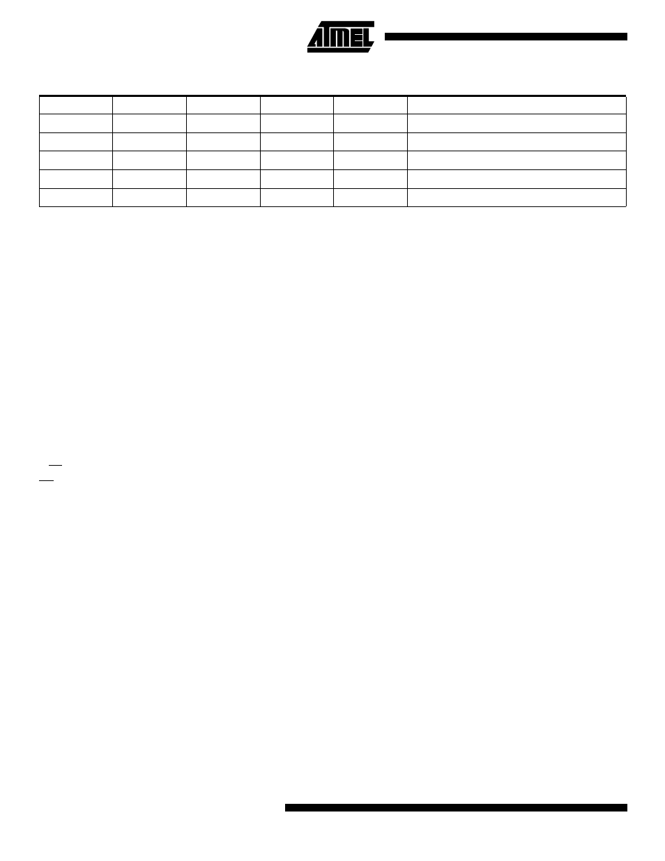
Table 45. DDBn Effects on Port B Pins
DDBn
PORTBn
PUD
I/O
Pull Up
Comment
0
0
x
Input
No
Tri-state (Hi-Z)
0
1
1
Input
No
Tri-state (Hi-Z)
0
1
0
Input
Yes
PBn will source current if ext. pulled low.
1
0
x
Output
No
Push-pull Zero Output
1
1
x
Output
No
Push-pull One Output