Timer/counter1 in pwm mode, Atmega163(l) – Rainbow Electronics ATmega163L User Manual
Page 41
ATmega163(L)
41
Since the Input Capture Register - ICR1 - is a 16-bit register, a temporary register TEMP is used when ICR1 is read to
ensure that both bytes are read simultaneously. When the CPU reads the low byte ICR1L, the data is sent to the CPU and
the data of the high byte ICR1H is placed in the TEMP register. When the CPU reads the data in the high byte ICR1H, the
CPU receives the data in the TEMP register. Consequently, the low byte ICR1L must be accessed first for a full 16-bit reg-
ister read operation.
The TEMP register is also used when accessing TCNT1, OCR1A, and OCR1B. If the main program and also interrupt rou-
tines accesses registers using TEMP, interrupts must be disabled during access from the main program and interrupt
routines.
Timer/Counter1 in PWM Mode
When the PWM mode is selected, Timer/Counter1 and the Output Compare Register1A - OCR1A and the Output Compare
Register1B - OCR1B, form a dual 8, 9, or 10-bit, free-running, glitch-free, and phase correct PWM with outputs on the
PD5(OC1A) and PD4(OC1B) pins. In this mode, the Timer/Counter1 acts as an up/down counter, counting up from $0000
to TOP (see Table 16), where it turns and counts down again to zero before the cycle is repeated. When the counter value
matches the contents of the 8, 9, or 10 least significant bits (depending on resolution) of OCR1A or OCR1B, the
PD5(OC1A)/PD4(OC1B) pins are set or cleared according to the settings of the COM1A1/COM1A0 or COM1B1/COM1B0
bits in the Timer/Counter1 Control Register TCCR1A. Refer to Table 12 on page 37 for details.
Alternatively, the Timer/Counter1 can be configured to a PWM that operates at twice the speed as in the mode described
above. Then the Timer/Counter1 and the Output Compare Register1A - OCR1A and the Output Compare Register1B -
OCR1B, form a dual 8, 9, or 10-bit, free-running and glitch-free PWM with outputs on the PD5(OC1A) and PD4(OC1B)
pins.
As shown in Table 15, the PWM operates at either 8, 9, or 10 bits resolution. Note the unused bits in OCR1A, OCR1B, and
TCNT1 will automatically be written to zero by hardware. I.e. bit 9 to 15 will be set to zero in OCR1A, OCR1B, and TCNT1
if the 9-bit PWM resolution is selected. This makes it possible for the user to perform read-modify-write operations in any of
the three resolution modes and the unused bits will be treated as don’t care.
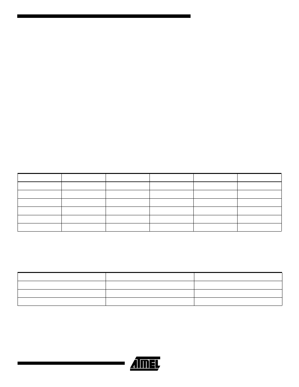
Table 15. Timer TOP Values and PWM Frequency
CTC1
PWM11
PWM10
PWM Resolution
Timer TOP Value
Frequency
0
0
1
8-bit
$00FF (255)
f
TCK1
/510
0
1
0
9-bit
$01FF (511)
f
TCK1
/1022
0
1
1
10-bit
$03FF(1023)
f
TCK1
/2046
1
0
1
8-bit
$00FF (255)
f
TCK1
/256
1
1
0
9-bit
$01FF (511)
f
TCK1
/512
1
1
1
10-bit
$03FF(1023)
f
TCK1
/1024
Table 16. Timer TOP Values and PWM Frequency
PWM Resolution
Timer TOP Value
Frequency
8-bit
$00FF (255)
f
TC1
/510
9-bit
$01FF (511)
f
TC1
/1022
10-bit
$03FF(1023)
f
TC1
/2046