Interrupt response time, The general interrupt mask register - gimsk, The general interrupt flag register - gifr – Rainbow Electronics ATmega163L User Manual
Page 27: Atmega163(l)
ATmega163(L)
27
Note that external level interrupt does not have a flag, and will only be remembered for as long as the interrupt condition is
present.
Note that the status register is not automatically stored when entering an interrupt routine and restored when returning from
an interrupt routine. This must be handled by software.
Interrupt Response Time
The interrupt execution response for all the enabled AVR interrupts is 4 clock cycles minimum. After 4 clock cycles the pro-
gram vector address for the actual interrupt handling routine is executed. During this 4 clock cycle period, the Program
Counter (13 bits) is pushed onto the Stack. The vector is normally a jump to the interrupt routine, and this jump takes 3
clock cycles. If an interrupt occurs during execution of a multi-cycle instruction, this instruction is completed before the
interrupt is served. If an interrupt occurs when the MCU is in sleep mode, the interrupt execution response time is
increased by 4 clock cycles.
A return from an interrupt handling routine takes 4 clock cycles. During these 4 clock cycles, the Program Counter (2 bytes)
is popped back from the Stack, the Stack Pointer is incremented by 2, and the I flag in SREG is set. When AVR exits from
an interrupt, it will always return to the main program and execute one more instruction before any pending interrupt is
served.
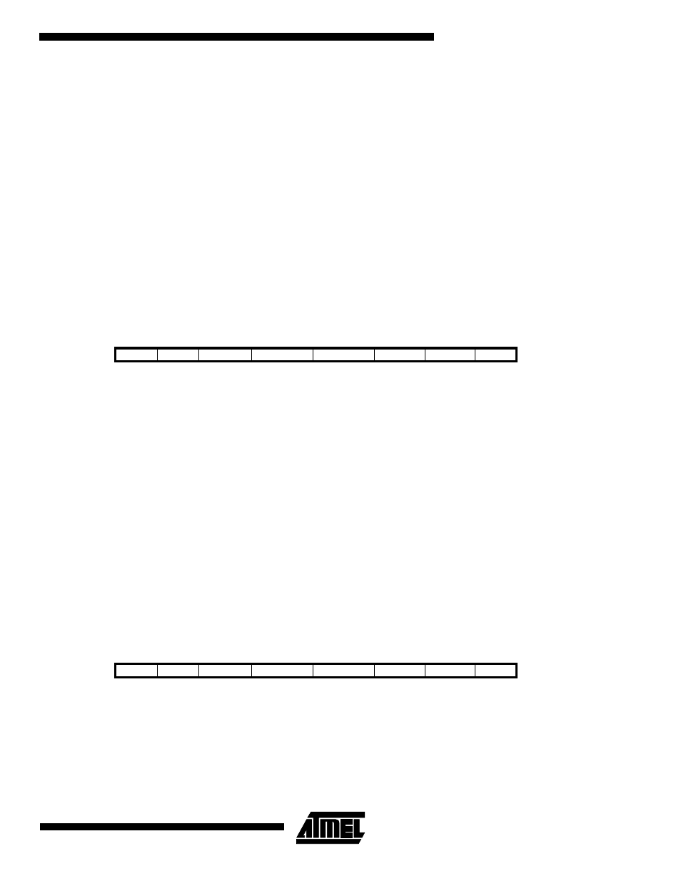
The General Interrupt Mask Register - GIMSK
•
Bit 7 - INT1: External Interrupt Request 1 Enable
When the INT1 bit is set (one) and the I-bit in the Status Register (SREG) is set (one), the external pin interrupt is activated.
The Interrupt Sense Control1 bits 1/0 (ISC11 and ISC10) in the MCU general Control Register (MCUCR) define whether
the external interrupt is activated on rising and/or falling edge of the INT1 pin or level sensed. Activity on the pin will cause
an interrupt request even if INT1 is configured as an output. The corresponding interrupt of External Interrupt Request 1 is
executed from program memory address $004. See also “External Interrupts”.
•
Bit 6 - INT0: External Interrupt Request 0 Enable
When the INT0 bit is set (one) and the I-bit in the Status Register (SREG) is set (one), the external pin interrupt is activated.
The Interrupt Sense Control0 bits 1/0 (ISC01 and ISC00) in the MCU general Control Register (MCUCR) define whether
the external interrupt is activated on rising or falling edge of the INT0 pin or level sensed. Activity on the pin will cause an
interrupt request even if INT0 is configured as an output. The corresponding interrupt of External Interrupt Request 0 is
executed from program memory address $002. See also “External Interrupts.”
•
Bits 5 - Res: Reserved Bits
This bit is reserved in the ATmega163 and the read value is undefined.
•
Bits 4..0 - Res: Reserved Bits
These bits are reserved bits in the ATmega163 and always read as zero.
The General Interrupt Flag Register - GIFR
•
Bit 7 - INTF1: External Interrupt Flag1
When an event on the INT1 pin triggers an interrupt request, INTF1 becomes set (one). If the I-bit in SREG and the INT1 bit
in GIMSK are set (one), the MCU will jump to the interrupt vector at address $004. The flag is cleared when the interrupt
routine is executed. Alternatively, the flag can be cleared by writing a logical one to it. This flag is always cleared when
INT1 is configured as a level interrupt.
Bit
7
6
5
4
3
2
1
0
$3B ($5B)
INT1
INT0
-
-
-
-
-
-
GIMSK
Read/Write
R/W
R/W
R
R
R
R
R
R
Initial value
0
0
x
0
0
0
0
0
Bit
7
6
5
4
3
2
1
0
$3A ($5A)
INTF1
INTF0
-
-
-
-
-
-
GIFR
Read/Write
R/W
R/W
R
R
R
R
R
R
Initial value
0
0
0
0
0
0
0
0