Timer/counter 0 - tcnt0, Bit timer/counter1, Atmega163(l) – Rainbow Electronics ATmega163L User Manual
Page 36
ATmega163(L)
36
Timer/Counter 0 - TCNT0
The Timer/Counter0 is implemented as an up-counter with read and write access. If the Timer/Counter0 is written and a
clock source is present, the Timer/Counter0 continues counting in the clock cycle following the write operation.
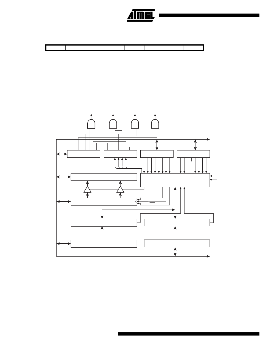
16-bit Timer/Counter1
Figure 33 shows the block diagram for Timer/Counter1.
Figure 33. Timer/Counter1 Block Diagram
The 16-bit Timer/Counter1 can select clock source from CK, prescaled CK, or an external pin. In addition it can be stopped
as described in section “Timer/Counter1 Control Register B - TCCR1B” on page 38. The different status flags (overflow,
compare match, and capture event) are found in the Timer/Counter Interrupt Flag Register - TIFR. Control signals are
found in the Timer/Counter1 Control Registers - TCCR1A and TCCR1B. The interrupt enable/disable settings for
Timer/Counter1 are found in the Timer/Counter Interrupt Mask Register - TIMSK.
When Timer/Counter1 is externally clocked, the external signal is synchronized with the oscillator frequency of the CPU. To
assure proper sampling of the external clock, the minimum time between two external clock transitions must be at least one
internal CPU clock period. The external clock signal is sampled on the rising edge of the internal CPU clock.
Bit
7
6
5
4
3
2
1
0
$34 ($54)
MSB
LSB
TCNT0
Read/Write
R/W
R/W
R/W
R/W
R/W
R/W
R/W
R/W
Initial value
0
0
0
0
0
0
0
0
8-BIT D
A
TA
B
U
S
T/C1 CONTROL
REGISTER B (TCCR1B)
T/C1 CONTROL
REGISTER A (TCCR1A)
T/C1 INPUT CAPTURE REGISTER (ICR1)
16 BIT COMPARATOR
16 BIT COMPARATOR
TIMER/COUNTER1 OUTPUT COMPARE REGISTER A
TIMER/COUNTER1 OUTPUT COMPARE REGISTER B
TIMER/COUNTER1 (TCNT1)
TIMER INT. FLAG
REGISTER (TIFR)
0
0
0
0
0
0
7
7
7
7
7
7
8
8
8
8
8
8
15
15
15
15
15
15
CONTROL
LOGIC
COM1A1
COM1B1
CS12
TO
V
1
TO
V
1
TO
V
0
OCF1A
OCF1A
OCF1B
OCF1B
ICF1
ICF1
COM1A0
COM1B0
CS1
1
CTC1
PWM1
1
PWM10
ICES1
ICNC1
CS10
CK
T/C1 COMPARE
MATCH A IRQ
T/C1 COMPARE
MATCH B IRQ
T/C1 INPUT
CAPTURE IRQ
T/C1 OVER-
FLOW IRQ
CAPTURE
TRIGGER
T/C CLOCK SOURCE
T/C CLEAR
UP/DOWN
TIMER INT. MASK
REGISTER (TIMSK)
T
O
IE0
T
O
IE1
OCIE1A
OCIE1B
TICIE1
T
O
IE2
TO
V
2
OCIE2
OCF2
FOC1A
FOC1B
T1