Asynchronous status register - assr, Atmega163(l) – Rainbow Electronics ATmega163L User Manual
Page 48
ATmega163(L)
48
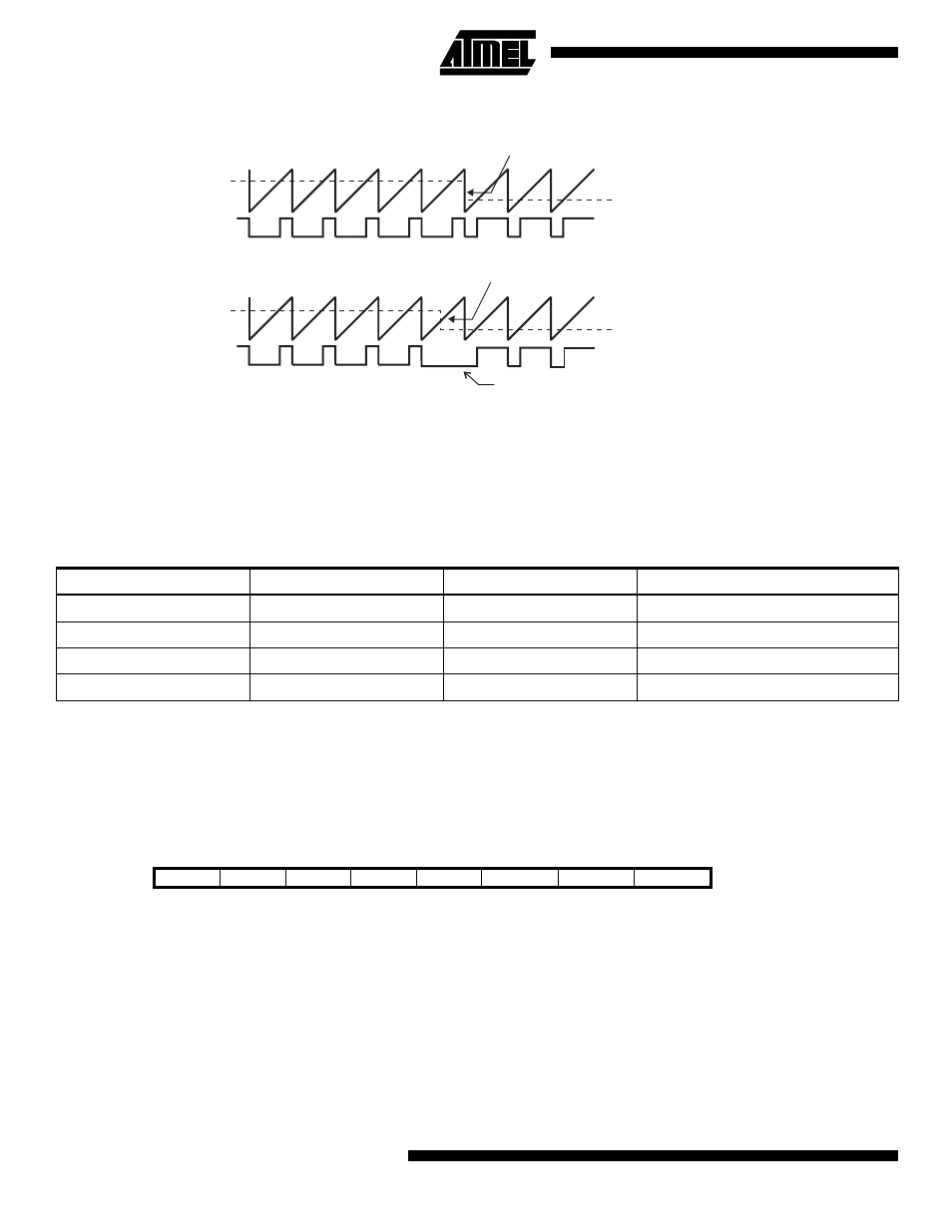
Figure 39. Effects of Unsynchronized OCR Latching in Overflow Mode.
During the time between the write and the latch operation, a read from OCR2 will read the contents of the temporary loca-
tion. This means that the most recently written value always will read out of OCR2.
When the Output Compare Register contains $00 or $FF, and the up/down PWM mode is selected, the output PD7(OC2) is
updated to low or high on the next compare match according to the settings of COM21/COM20. This is shown in Table 22.
In overflow PWM mode, the output PD7(OC2) is held low or high only when the Output Compare Register contains $FF.
In up/down PWM mode, the Timer Overflow Flag - TOV2, is set when the counter changes direction at $00. In overflow
PWM mode, the Timer Overflow Flag is set as in normal Timer/Counter mode. The Timer Overflow Interrupt operates
exactly as in normal Timer/Counter mode, i.e. it is executed when TOV2 is set provided that Timer Overflow Interrupt and
global interrupts are enabled. This also applies to the Timer Output Compare flag and interrupt.
The frequency of the PWM will be Timer Clock Frequency divided by 510.
Asynchronous Status Register - ASSR
•
Bit 7..4 - Res: Reserved Bits
These bits are reserved bits in the ATmega163 and always read as zero.
•
Bit 3 - AS2: Asynchronous Timer/Counter2
When AS2 is cleared (zero), Timer/Counter2 is clocked from the internal system clock, CK. When AS2 is set (one),
Timer/Counter2 is clocked from the PC6(TOSC1) pin. Pins PC6 and PC7 are connected to a crystal oscillator and cannot
be used as general I/O pins. When the value of this bit is changed, the contents of TCNT2, OCR2, and TCCR2 might be
corrupted.
Table 22. PWM Outputs OCR2 = $00 or $FF
COM21
COM20
OCR2
Output OC2
1
0
$00
L
1
0
$FF
H
1
1
$00
H
1
1
$FF
L
Bit
7
6
5
4
3
2
1
0
$22 ($22)
-
-
-
-
AS2
TCN2UB
OCR2UB
TCR2UB
ASSR
Read/Write
R
R
R
R
R/W
R
R
R
Initial value
0
0
0
0
0
0
0
0
PWM Output OC2
PWM Output OC2
Unsynchronized OC2 Latch
Synchronized OC2 Latch
Counter Value
Compare Value
Counter Value
Compare Value
Compare Value changes
Compare Value changes
Glitch