Port d, The port d data register - portd, The port d data direction register - ddrd – Rainbow Electronics ATmega163L User Manual
Page 110: The port d input pins address - pind, Port d as general digital i/o, Atmega163(l)
ATmega163(L)
110
Port D
Port D is an 8 bit bi-directional I/O port with internal pull-up resistors.
Three I/O memory address locations are allocated for Port D, one each for the Data Register - PORTD, $12($32), Data
Direction Register - DDRD, $11($31) and the Port D Input Pins - PIND, $10($30). The Port D Input Pins address is read
only, while the Data Register and the Data Direction Register are read/write.
The Port D output buffers can sink 20 mA. As inputs, Port D pins that are externally pulled low will source current if the pull-
up resistors are activated. Some Port D pins have alternate functions as shown in Table 48.
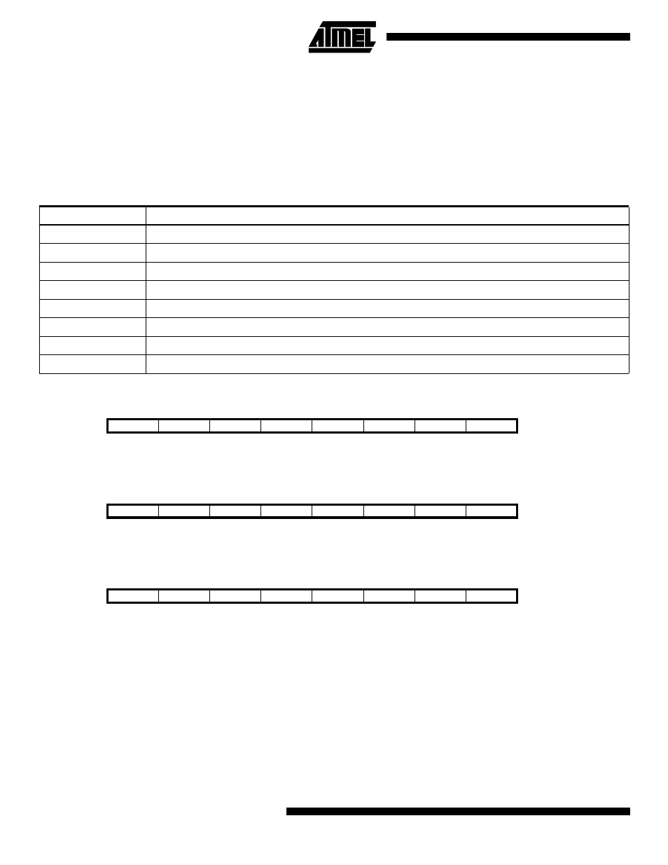
The Port D Data Register - PORTD
The Port D Data Direction Register - DDRD
The Port D Input Pins Address - PIND
The Port D Input Pins address - PIND - is not a register, and this address enables access to the physical value on each
Port D pin. When reading PORTD, the PORTD Data Latch is read, and when reading PIND, the logical values present on
the pins are read.
Port D As General Digital I/O
PDn, General I/O pin: The DDDn bit in the DDRD register selects the direction of this pin. If DDDn is set (one), PDn is con-
figured as an output pin. If DDDn is cleared (zero), PDn is configured as an input pin. If PDn is set (one) when configured
as an input pin the MOS pull up resistor is activated. To switch the pull up resistor off the PDn has to be cleared (zero), the
Table 48. Port D Pins Alternate Functions
Port Pin
Alternate Function
PD0
RXD (UART Input Pin)
PD1
TXD (UART Output Pin)
PD2
INT0 (External Interrupt 0 Input)
PD3
INT1 (External Interrupt 1 Input)
PD4
OC1B (Timer/Counter1 Output CompareB Match Output)
PD5
OC1A (Timer/Counter1 Output CompareA Match Output)
PD6
ICP (Timer/Counter1 Input Capture Pin)
PD7
OC2 (Timer/Counter2 Output Compare Match Output)
Bit
7
6
5
4
3
2
1
0
$12 ($32)
PORTD7
PORTD6
PORTD5
PORTD4
PORTD3
PORTD2
PORTD1
PORTD0
PORTD
Read/Write
R/W
R/W
R/W
R/W
R/W
R/W
R/W
R/W
Initial value
0
0
0
0
0
0
0
0
Bit
7
6
5
4
3
2
1
0
$11 ($31)
DDD7
DDD6
DDD5
DDD4
DDD3
DDD2
DDD1
DDD0
DDRD
Read/Write
R/W
R/W
R/W
R/W
R/W
R/W
R/W
R/W
Initial value
0
0
0
0
0
0
0
0
Bit
7
6
5
4
3
2
1
0
$10 ($30)
PIND7
PIND6
PIND5
PIND4
PIND3
PIND2
PIND1
PIND0
PIND
Read/Write
R
R
R
R
R
R
R
R
Initial value
N/A
N/A
N/A
N/A
N/A
N/A
N/A
N/A