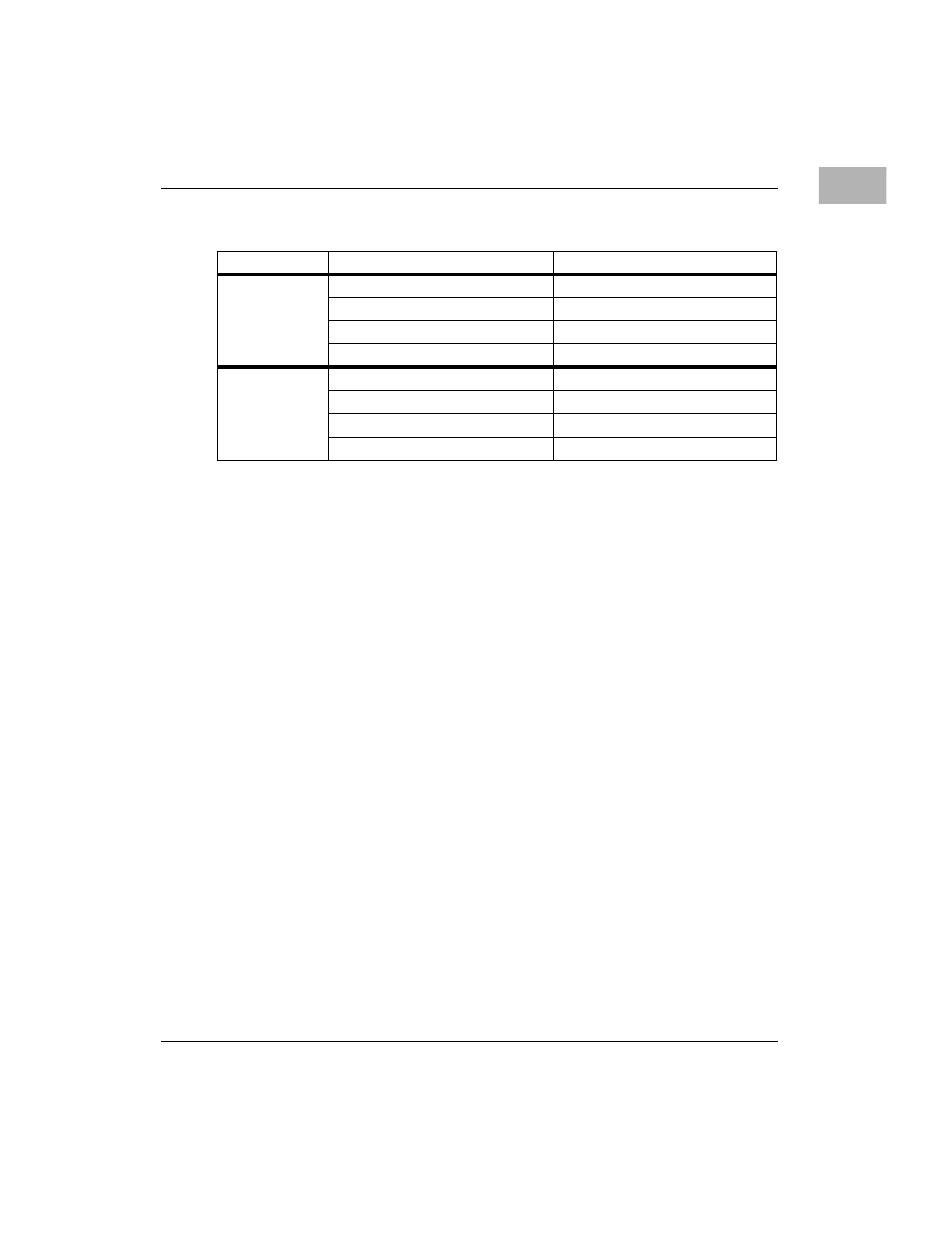
Table 1-12. z85230 scc register addresses -37, Table 1-12 – Motorola MVME172 User Manual
Page 55

Memory Maps
http://www.mcg.mot.com/literature
1-37
1
Note
A bug in MVME172s that have MC2 chip revision $01 does
not allow the data registers to be accessed directly. You must
access them indirectly via the SCC chip. The software must
send a command to the control register that tells it that the
next thing read or written to the control register will go to the
data register. The following two macros are examples:
dev_addr
is a pointer to the base address of the SCC.
SCCR0
is the offset to the SCC control register #0.
#define READ_SCC(VAR_NAME)\
dev_addr[SCCR0] = 0x08;\
(VAR_NAME) = dev_addr[SCCR0]
#define WRITE_SCC(VAR_NAME)\
dev_addr[SCCR0] = 0x08;\
dev_addr[SCCR0] = (VAR_NAME)
Table 1-12. Z85230 SCC Register Addresses
SCC
Z85230 SCC Register
Address
SCC #1
(All MVME172
modules)
Port B Control
$FFF45001
Port B Data
$FFF45003
Port A Control
$FFF45005
Port A Data
$FFF45007
SCC #2
(200/300-Series
MVME172
only)
Port B Control
$FFF45801
Port B Data
$FFF45803
Port A Control
$FFF45805
Port A Data
$FFF45807
