Z85230 scc interface, Z85230 scc interface -6, Table 3-1. dram performance -6 – Motorola MVME172 User Manual
Page 194
3-6
Computer Group Literature Center Web Site
MC2 Chip
3
Note
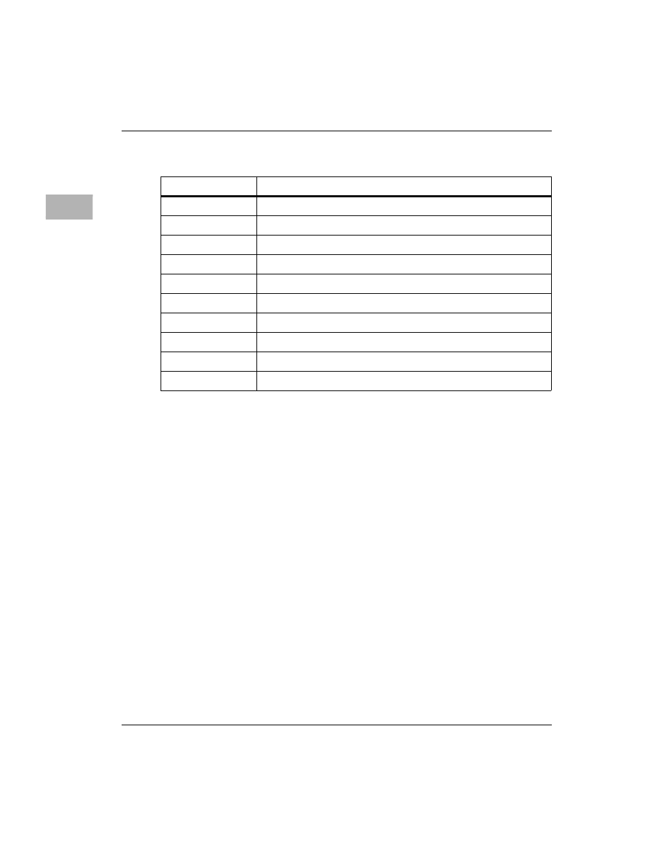
TEA is the MC68060 bus error transaction signal. “With
TEA” indicates that a bus error cycle occurs if a DRAM
parity error was detected.
Z85230 SCC Interface
The MC2 chip provides a map decoder and an interrupt handler for the two
Zilog Z85230s. The base addresses are $FFF45000 and $FFF45800. The
MC2 chip requests an interrupt at the level programmed in the SCC
interrupt control register if the interrupt is enabled and a low level is
detected on the SCC INT* pin. The Z85230 provides the interrupt vector
for the interrupt acknowledge cycle. During the interrupt acknowledge
cycle, interrupts from the first Z85230 have priority over those from the
second Z85230.
The MC2 chip supports as many as four Z85230 devices. (There are two
Z85230s on the MVME172. Refer to the Board Level Hardware
Description in your MVME172 installation and use manual.) The
Table 3-1. DRAM Performance
Clock Budget
Operating Conditions
4,2,2,2
Non-interleaved, read, 25 MHz, without TEA on parity error
4,1,1,1
Interleaved, read, 25 MHz, without TEA on parity error
5,3,3,3
Non-interleaved, read, 25 MHz, with TEA on parity error
5,2,2,2
Interleaved, read, 25 MHz, with TEA on parity error
3,2,2,2
Write, 25 MHz
5,3,3,3
Non-interleaved, read, 32 MHz, without TEA on parity error
5,2,2,2
Interleaved, read, 32 MHz, without TEA on parity error
6,4,4,4
Non-interleaved, read, 32 MHz, with TEA on parity error
6,3,3,3
Interleaved, read, 32 MHz, with TEA on parity error
4,2,2,2
Write, 32 MHz